Analog Front Ends IP for TSMC
Welcome to the ultimate
Analog Front Ends IP
for
TSMC
hub! Explore our vast directory of
Analog Front Ends IP
for
TSMC
All offers in
Analog Front Ends IP
for
TSMC
Filter
Compare
32
Analog Front Ends IP
for
TSMC
from
6
vendors
(1
-
10)
-
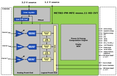
Complete measurement analog front end (AFE) IP for single phase power metering in TSMC 40ULP
- Embedded Computation Engine for utility billing applications
- Low noise Programmable Gain Amplifier (PGA), to reach the best class accuracy with each type of sensors
- Embedded power management for the best resilience to power supply noise
-
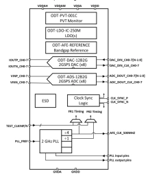
Ultra Low-Power High-Performance AFE on 12nm
- The ODT-AFE-4T4R-12nm is an ultra-high-performance AFE designed in a 12nm CMOS process.
- The AFE includes 2 IQ Pairs of Tx and Rx for the FR2 band, and combines them with 2 additional IQ Pairs of Tx and Rx for the FR1 band clocked at a lower sample rate.
-
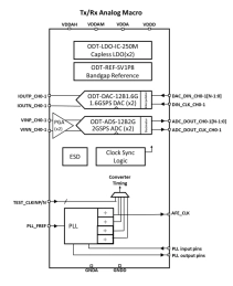
Ultra Low-Power High-Performance AFE in 12nm
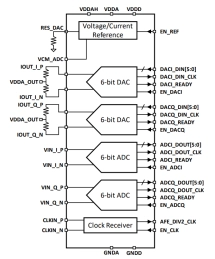
- The ODT-AFE-1T1R-12 is an ultra-high-performance AFE designed in a 12nm process.
- The AFE includes 1 IQ Pairs of Tx and Rx for either the FR1 or FR2 band. This is comprised of two 12-bit 2GSPS ADCs, and two 12-bit 2GSPS DACs.
- This AFE also includes multiple capless LDOs, a voltage/current reference, and a low jitter 2 GHz PLL
-
6-bit, 1 GSPS High Performance AFE in 28nm CMOS
- The ODT-AFE-6B1G-28HPCPT is a highperformance I/Q ADC and I/Q DAC designed in a 28nm CMOS process.
- The 6-bit, 1.056GSPS I/Q ADC supports input signals up to 400 MHz and features a differential full-scale range of 0.6Vpp and excellent static and dynamic performance.
- The ADC architecture is optimized to maximize performance while minimizing power and area consumption.
-
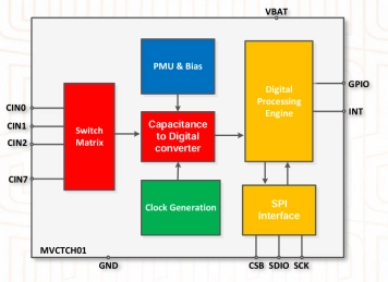
8-Channel Ultra-Low Power Capacitive Touch Interface
- The MVCTCH01 ASIC is an ultra-low power and high-sensitivity 8-channel capacitive touch interface that is designed to be easily integrated with capacitive touch pads.
- Ultra-low power operation is achieved by using a novel capacitive-to-digital converter, making it suitable for battery powered and portable devices.
-
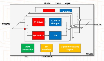
Ultrasound AFE Transceiver Chip for CMUT Transducers
- The MVUS01 ultrasound transducer interface is the first generation of high-voltage (HV) ultrasound ASICs intended for portable medical imaging probes and other markets.
- The chip supports pulsing ultrasonic transducers, with excitation voltages of up to 50V, and has high gain and low noise receivers, for increased sensitivity to ultrasonic echoes.
-
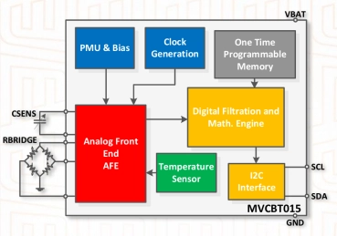
Digital Capacitive Plus Bridge Sensor Interfaces
- The MVCBT015 is a programmable, highly accurate, capacitance-to-digital converter and bridge interface that is designed to be easily integrated with capacitive and bridge sensors.
- The chip features very fast measurement times, low operating power, and very low standby currents, making it very suitable for low power and portable applications.
-
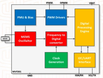
Frequency-to-Digital Converter for MEMS Resonators
- The MVFD01 is a programmable frequency-to-digital converter that is designed to be easily integrated with MEMS resonators.
- The chip features a versatile low noise amplifier (LNA) with a programmable gain and feedthrough capacitance cancellation, in order to accommodate different MEMS resonators
-
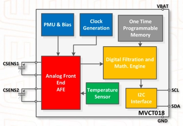
Dual Channel Digital Capacitive Sensor Interface
- The MVCT018 is a programmable and very accurate capacitance-to-digital converter interface, designed to be easily integrated with capacitive sensors.
- The chip features very fast measurement times, low operating power, and very low standby currents, making it very suitable for low power and portable applications.
-
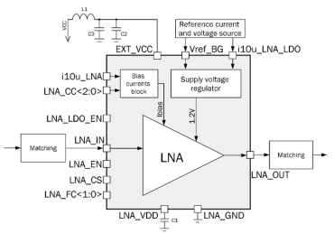
25 to 500 MHz LNA with 0.8 dB NF and 19 dB gain
- TSMC CMOS 55nm
- Operating frequency range from 25 to 500 MHz
- Low noise figure (0.8 dB)
- Gain control range 19 dB