The low-power wide range PLL addresses markets and applications that demand very low power and optimized for area efficiencies. In addition, consumer devices have restrictions on supply voltage due to battery restrictions or board restrictions. The PLLs also needs to be designed on standard digital logic processes and expected to work in noisy SoC environments.
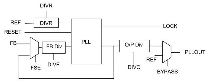
The PLL macro is implemented in Analog Bits’ proprietary architecture that uses core supply only. The PLL resides inside the IO ring that includes two analog power supply pads, occupying no core area. In order to minimize noise coupling and maximize ease of use, the PLL incorporates a proprietary ESD structure, which is proven in several generations of processes. Eliminating band-gaps and integrating all on-chip components such as capacitors and ESD structures, helps the jitter performance significantly and reduces stand-by power. The PLL macro fits into any standard IO pad pitch and can be implemented in staggered and in-line IO configurations.
PLL Operational Range Description Symbol Min Typ Max Units Input Frequency FREF 5 140 MHz Post-Divide Reference Frequency FPFD 5 140 MHz VCO Frequency FVCO 800 MHz Output Frequency FOUT 12.5 400 MHz Output Duty Cycle tDO 45 55 % Total area of macro (excluding bond pad area) A 0.024 sq. mm May vary depending on size of IO slots Chip core area requirement CA 0 sq. mm Total Power IDD 0.8 mA Operational Voltage (Digital) VDIG 1.08 1.2 1.32 V Operational Voltage (Analog) VANA 1.08 1.2 1.32 V Operational Temperature TOP -40 25 125 C Table 1: PLL Operational Range