Overview
A <4Gbps, Wide I/O Compatible, Die to Die Interface in TSMC 16nm and 28nm.
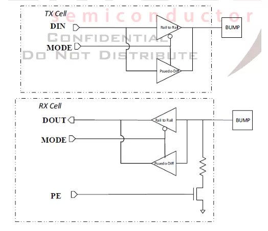
This silicon proven die to die interface includes IP in both TSMC 16nm FFC/FFC+ and 28nm HPM/HPC/HPC+. The I/O cells for both versions of the library are defined as TX only and RX only. The cells have two modes of operation: standard full rail to rail swing or a custom low noise psuedo-differential interface. The RX cells have a weak pull-down feature. The library is designed for Flip-chip/Die to Die packaging only, with no Wirebond option. Both library options have a common power bus architecture that when the cells are abutted, will feed through. There are no Power or Ground Pad/Cells, however all VDD and VSS connections will be made to the Core domain in upper metals. Both library options are ultra-low power, have a small footprint, MCM compliant, and have HBM & CDM robustness.
Operating Conditions for 16nm
| Parameter |
Value |
| VDDIO |
0.8V |
| I/O Device |
1.8V |
| Core |
Use SVT Only |
| Cell Size |
50x28.06um |
| BEOL |
M8 & below |
| VDD Core |
0.8V +/- 10% |
| Temperature |
-40C to 125C |
| Operational Bit Rate |
2Gbps1 |
Operating Conditions for 28nm
| Parameter |
Value |
| VDDIO |
0.9V |
| I/O Device |
1.8V |
| Core |
Use SVT Only |
| Cell Size |
50x25um |
| BEOL |
M8 & below |
| VDD Core |
0.9V +/- 10% |
| Temperature |
-40C to 125C |
| Operational Bit Rate |
2Gbps1 |
Cells for 16nm D2D
| Cell Name |
Width |
Description |
| UF_TX |
50x25um |
TX Cell |
| UF_RX |
50x25um |
RX Cell |
Cells for 28nm D2D
| Cell Name |
Width |
Description |
| UD_TX |
50x30.5um |
TX Cell |
| UD_RX |
50x30.5um |
RX Cell |
Learn more about Custom IP core
The growing adoption of RISC-V in high-performance and scientific computing has increased the need for performance-portable code targeting the RISC-V Vector (RVV) extension. However, current compiler infrastructures provide limited end-to-end support for generating optimized RVV code from high-level representations to low-level implementations. In particular, existing MLIR distributions lack practical lowering paths that map high-level abstractions to RVV intrinsics, limiting their applicability for production-ready RISC-V kernels. This paper presents a compilation approach that combines MLIR with xDSL to bridge the missing lowering stages required for RVV code generation.
As AI workloads scale exponentially, bandwidth has become the new bottleneck. This article explores how Celestial AI’s Photonic Fabric™ redefines interconnect performance, and how Sofics’ low-cap ESD and power clamp IP enabled its integration on TSMC’s 5nm platform.
See how Codasip Studio enables SYCLOPS to implement a customizable RISC-V Vector processor, accelerating the future of open-source, high-performance AI compute at the Edge.
The era of universal processor architectures is giving way to workload-specific designs optimized for performance, power, and scalability. As data-centric applications in artificial intelligence (AI), edge computing, automotive, and industrial markets continue to expand, they are driving a fundamental shift in processor design.
The authors introduce a HW/SW co-design toolset capable of adapting to a user-defined architecture description that captures the instruction set extension semantics.
When designing complex Systems-on-Chip, software teams should be involved early in the process. This will help identify architectural bottlenecks, validate system behavior, and accelerate the entire project timeline. In this process, processor simulation models play a crucial role.