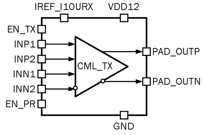
065TSMC_CML_02 core logic interface includes signal pins (INP1, INP2 and INN1, INN2) for data transmission, control pin EN_TX to configure transmitter state and control pin EN_PR to toggle pre-emphasis mode. Data on signal pins INP2 and INN2 should be one bit shifted (delayed) from that on INP1 and INN1 for pre-emphasis purposes. Differential CML output pins PAD_OUTP and PAD_OUTN should be connected to bonding pads.
3.125 Gbps DDR 1-channel CML transmitter
Overview
Key Features
- TSMC CMOS 0.065 um
- 1.2 V digital power supply
- 1.2 V CMOS output logic signals
- 8-step (3-bit) adjustable transmitter output current (range from 4 mA to 32 mA)
- 3.125 Gbps (DDR MODE) switching rates
- Temperature range: -40 °C to + 125 °C
- Optimized for pad-limited layout design
- Portable to other technologies (upon request)
Block Diagram
Applications
- Point-to-point data transmission
- Multidrop buses
- Clock distribution
- Backplane receiver
- Backplane data transmission
- Cable data transmission
Deliverables
- Schematic or NetList
- Abstract model (.lef and .lib files)
- Layout view (optional)
- Behavioral model (Verilog)
- Extracted view (optional)
- GDSII
- DRC, LVS, antenna report
- Test bench with saved configurations (optional)
- Documentation
Technical Specifications
Short description
3.125 Gbps DDR 1-channel CML transmitter
Vendor
Vendor Name
Foundry, Node
TSMC CMOS 65 nm
Maturity
silicon proven
Availability
Now
TSMC
Silicon Proven:
65nm
G