DLL IP
Welcome to the ultimate DLL IP hub! Explore our vast directory of DLL IP.
DLL stands for Delay Locked Loops. A Delay Locked Loop IP core refers to a digital feedback circuit wherein there is no use of an oscillator, but instead a delay line is employed as the output is phase locked to an input.
All offers in
DLL IP
Filter
Compare
719
DLL IP
from
11
vendors
(1
-
10)
-
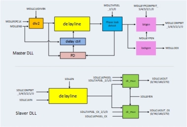
Master/Slave DLL
- The (Delay-Locked Loop) DLL PHY is a mix-signal circuit used in low-power and high-speed applications to align and synchronize clock signals with precise timing
- This IP ensures robust timing, minimizes skew, and operates efficiently with a small silicon footprint
- The DLL PHY is designed to generate precise phase-shifted clocks (e.g
- 0 ° , 90 ° , 180 °, 270 °) based on a reference clock, enabling high-speed data capture and transmission
-
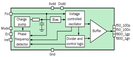
800/1000 MHz DLL-based frequency multiplier
- TSMC 90 nm CMOS
- Low jitter
- Precisely aligns the clock distribution output with a reference clock
- Low current consumption
-
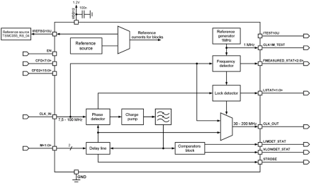
30-200 MHz DLL-based frequency multiplier
- TSMC CMOS 55 nm
- 30 – 200 MHz output frequency
- 7.5 – 100 MHz reference frequency
- Multiplication factor 1, 2, 3 or 4
- Glitch-free mode switching
-
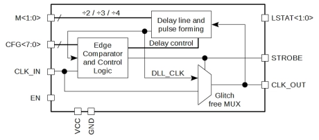
10 to 200 MHz DLL-based frequency multiplier
- Global Foundries CMOS 55 nm
- 10 – 200 MHz output frequency
- 0.01 – 100 MHz reference frequency
- Glitch-free mode switching
-
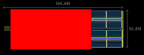
CC-100IP-PI Power Integrity Enhancement IP
- Occupies the same on chip area as standard DCAPs with at least a 600X effective capacitance increase
- Up to a 36% Dynamic Power and RF Emissions Reduction
- On-Chip Cybersecurity Enhancement
- 25% Reduction in Capacitor ESL
-
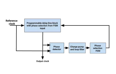
Delay Locked Loop IP
- Timing resolution: 80ps
- Operating frequency range: 160MHz – 700 MHz
- Lock time: 11 cycles
- Generates user configurable precise phase shifts from 00 to 3600 with a resolution of 10
-
DDR DLL
- High Precision DLL
- Provision of both coarse and fine controls to minimize resolution error
- External bypass and check of generated delay code
-
DLL
- Precise Clock Alignment: Ensures accurate clock timing by adjusting delays to match the reference clock
- Low Jitter: Minimizes phase noise and jitter, crucial for high-speed data communication and processing
- Programmable Delay: Offers flexibility with programmable delay settings, allowing easy customization
- Low Power Consumption: Optimized for minimal power usage, suitable for energy-sensitive applications
-
800Mb/s DDR DLL on TSMC CLN55LP
- Generates precise degrees of clock phase shifting for mobile or standard DDR applications
- Phase adjustments of non-continuous strobe clocks
- Compensates for external clock and data delays
- Programmable delay for precise and granular control of delay
-
UMC L90SP 90nm DDR DLL - 60MHz-300MHz
- Designed for high-speed DDR style interface applications.
- Generates precise delays that can be programmed from 0 to 360 degrees of the reference period.
- Delays multiple periodic or aperiodic signals independent of voltage and temperature.
- Delivers optimal jitter performance over a wide frequency range.