Using ARM Processor-based Flash MCUs as a Platform for Custom Systems-on-Chip
By Peter Bishop, CommunicationsManager,
Atmel Rousset
Abstract
Advances in process technology are making it possible to fabricate systems-on-chip (SoCs) containing hundreds of millions of transistors operating at gigahertz clock frequencies in a few tens of square millimeters. However, these same advances are making it increasingly difficult to develop such complex SoCs economically in an acceptable timescale, and making power consumption a critical issue. Yield and testability issues are becoming a major concern. SoCs incorporate programmable elements (microcontrollers (MCUs) and digital signal processors (DSPs)) making their software content as expensive and time-consuming to develop as their hardware.
Using a Flash MCU based on the industrystandard ARM processor as a platform represents a practical approach to SoC development that addresses all these issues. Incorporating an FPGA (field programmable gate array) prototyping step into the design flow enables parallel hardware/software testing and increases the chances of right-first-time silicon.
The Big Picture: System-on-Chip Challenges
There is a consensus in the semiconductor industry that the challenges facing designers of systems-on-chip (SoC) are electronic system level (ESL) design, design for manufacturing (DFM)/design for test (DFT), power management, and the cost, time and risk associated with SoC development. As a consequence of these challenges, there has been a decrease in recent years in the number of systems-on-chip being designed, offset by the increase in revenue derived from a successful system-onchip. embedded MCU market and has truly earned the title of “8051 of the this generation”.
Electronic System Level Design
A system-on-chip is almost always built around one or more microcontroller(s) (MCUs), digital signal processing (DSP) core(s) or other software programmable element. Accordingly, the software that drives the system must be developed concurrently with the hardware, and is at least as costly and time-consuming.
Numerous attempts are being made to develop a unified language to specify the entire SoC (both hardware and software) at the outset of the design cycle. These electronic system level (ESL) design projects are mostly based on System Verilog or System C, but to date neither has been widely adopted in practice. In reality most SoC hardware and software is developed concurrently but separately. This causes a number of problems, originating from the differences in culture, training and methodology between hardware and software developers. Combined hardware/ software testing only occurs late in the design cycle, and the hardware/software interface is a major source of errors. In addition architectural limitations or design errors are often detected late in the cycle.
It is recognized that ESL design is essential in reducing the time-to-market of the end-user product.
Design for Manufacturing
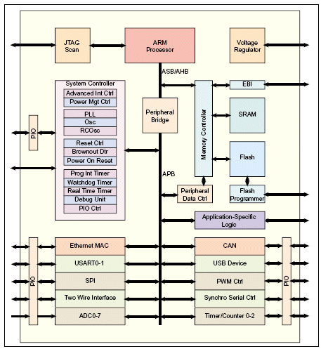
Figure 1: System-on-Chip with embedded MCU and Memory Blocks
Design for manufacturing (DFM) implies taking into account issues that influence yield and device characteristics during the logical and physical phases of the design cycle. It involves “feeding forward” process issues into design steps that have traditionally been process-independent. The first area to be impacted has been timing closure and the identification of critical signal paths. Physical synthesis has been helpful in addressing this, but is not a panacea.
Analog characterization is a major area of difficulty, as is that of embedded Flash memory. The process compromises required in embedding Flash into mainstream CMOS technology give rise to problems of endurance/data retention. There is also the practical issue of the time take for Flash programming, often carried out as an integral part of the test cycle. Yield optimization is generally carried out by process refinement after successive iterations of a product once it is in volume production. This can be expensive unless an acceptable yield level is achieved reasonably rapidly.
Design for Test
Design for test (DFT) is well understood for digital logic, where scan insertion/automatic test pattern generation (ATPG) is the norm. Built-in self-test (BIST) for embedded memories is less common now than a decade ago. Accordingly, the time taken in testing of embedded Flash memory can be a major issue unless adequate provisions such as parallel testing are made.
Power Management
Wasted power drains supplies by generating heat, both of which are undesirable. The problem is becoming more significant with smaller transistor geometries, in particular static leakage current due to reduced gate thickness. Higher clock speeds lead to a proportional increase in dynamic power consumption.
A number of approaches to power management are in vogue, including partitioning the device into separate voltage islands and clock domains. These enable the clock to be slowed or stopped in under- or unused blocks (to reduce dynamic power consumption), and unused blocks to be powered down (to reduce static power consumption).
In extreme cases the entire SoC can be put in power-down mode except for its real-time clock, but the time taken to wake up from low-power mode can be an issue. It is essential to integrate a device-wide power management methodology into the design of an SoC from the outset; it cannot be grafted on as an afterthought.
Development Cost, Time and Risk
These are all becoming more significant with smaller geometries: mask costs are escalating (although they reduce once a process becomes stable), design times are lengthening in proportion to the transistor count, and increasing design complexity makes errors more difficult to detect during the design flow. Hardware/software interaction is an increasing source of error, and difficult to identify until late in the design flow. The delay and cost over-run induced by a re-spin can kill a product. Often the market window has closed, particularly for a consumer product, and client dissatisfaction can lead to cancelled orders or worse.
An ARM-based Flash Microcontroller as an Architecture Platform
Using an ARM-based Flash microcontroller as an architecture platform for the development of a custom (application-specific) SoC is a practical approach that addresses all the challenges outlined in the previous sections. It takes advantage of available design methodologies and fabrication technologies, while giving a higher performance than the previous approach of testchips-plus-FPGA for dedicated logic. It enables parallel hardware and software development, with the additional advantage of software implementation on embedded Flash (as opposed to ROM) that facilitates bug fixes and upgrades to meet evolving interface standards. The design cycle is short (months instead of years for an SoC designed from scratch) and the extensive re-use of IP blocks makes it costeffective. It is an approach based on years of experience and multiple successful SoC products.
ARM-based Flash MCU Platform
ARM-based Flash MCU Platform Architecture
The general-purpose architecture of an ARM-based MCU platform (Figure 2) is characterized by a high level of system integration. It embeds an ARM processor core together with Flash memory for program and reference data storage and an SRAM workspace. An external bus interface (EBI) provides high-speed access to external memories or memory-mapped devices such as FPGAs to emulate custom logic.
The system controller includes a number of elements that until recently were off-chip, notably oscillator/PLL, voltage regulator, reset controller, brownout detector and power-on-reset. An advanced interrupt controller (AIC) reduces interrupt latency, enhancing the real-time performance of the system. The system controller also includes the power management controller that is the central clock source to the entire device.
External communication is via industrystandard interfaces such as USB, SPI, etc. Data throughput is enhanced by peripheral DMA controller (PDC) channels that link each external interface directly with the memory, enabling data transfers to take place with no processor intervention.
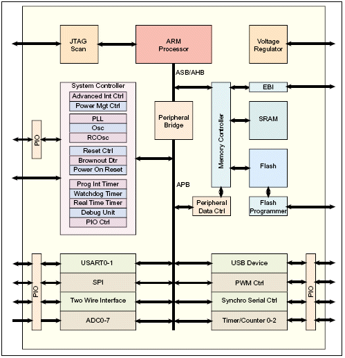
Figure 2: ARM-based Flash MCU Platform Architecture
A multi-channel ADC enables sensors and other analog devices to be directly connected. A parallel I/O controller multiplexes the input/outputs from the communications interfaces with a number of generalpurpose I/O lines, significantly reducing the device pin count.
Modular AMBA-compliant IP Blocks
The intellectual property (IP) blocks that make up the ARM-based SoC are all separately designed, validated and documented. They are designed for re-use, either inhouse or externally by qualified sub-contractors. They are characterized on-silicon, in particular the characteristics of the analog and Flash memory blocks are determined. Software device drivers, real-time operating systems and communications protocol stacks are developed and tested in parallel. The industry-standard ARM core facilitates software development via the reuse of legacy code and the availability of a wide range of software development tools, ported operating systems and support.
Synthesized, Fabricated and Characterized Platform
The ARM-based Flash MCU platform is created by integrating the qualified IP blocks around the ARM core. The platform is synthesized, timing closure is achieved, critical paths are dealt with and power consumption is optimized by fabricating the device and marketing it as a standard product, with successive silicon iterations for yield enhancement. The device is validated in multiple applications by diverse clients.
Transformation to Application- Specific System-on-Chip
The generic ARM-based Flash MCU platform is transformed into an application-specific device (Figure 3) by adding or removing communications interfaces, and by building in an application-specific logic block. The EBI or one of the high-speed serial interfaces is used to connect external memory-mapped devices. Data throughput is enhanced by the DMA capability that reduces processor performance loss to a few percent during bulk data transfers. The application-specific SoC is emulated on an FPGA-based development platform before fabrication, as described in a later section.
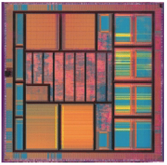
Figure 3: Application-specific SoC Derived from
SoC Design Flow based on Architecture and Emulation Platforms
The System-on-Chip design flow shown in Figure 4 is based on parallel hardware and software development. Its starting point is the architecture platform pre-built from generic hardware and software IP blocks that have already been characterized and debugged, as described in previous sections. The key steps are to partition the hardware and software of the application-specific system, using the existing hardware/software IP blocks as a guide. Then follows the development of any application-specific hardware and software IP blocks that are required. These are integrated, together with an operating system if needed, into the architecture platform and associated software. After synthesis and simulation, the hardware and software of the application- specific system are emulated on an FPGA-based emulation platform.

Figure 4: SoC Design Flow
Emulation Platform Architecture
The central feature of the emulation platform (Figures 5 and 6) is a high-density FPGA onto which are mapped the application- specific logic and any non-standard communications interfaces. An on-board clock generator provides all the required timing sources. There are connections to mezzanine board(s) that host the architecture platform(s), and both on-board and external memories. There are also connections to custom interface boards, and an extensive set of user switches, displays, LEDs and buttons. There are interfaces (including PHYs) for USB, Ethernet, RS232 and other standards, as well as external user I/O pins.
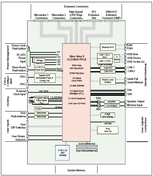
Figure 5: Emulation Platform Architecture
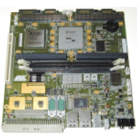
Figure 6: Atmel’s Mistral Emulation Platform
Emulation Key Steps
The first step is to map the Verilog or VHDL code of the application-specific IP block and any non-standard communications interfaces onto the FPGA. The architecture platform(s) are available on plug-in mezzanine boards (Figure 7). These, and any custom interface boards are connected to the emulation platform, which is in turn linked to the development PC.

Figure 7: Mezzanine Board for ARM Core-based Architecture Platform
The development software, comprising at least the low-level device drivers, operating system and basic functional modules, is loaded on the PC, from where it is run and debugged using an industry-standard development system. Although the emulation board cannot generally achieve the full operational speed of the target device, it is orders of magnitude faster than a simulation, and enables functional behavior to be investigated, rather than just simulation test patterns.
Should any errors be detected, they are corrected either by modifications to the Verilog/VHDL code of the IP blocks, or by modifications to the device drivers or higher- level software. The sequence of test/correction continues until all errors have been identified and eliminated.
Emulation Benefits
Emulation provides many benefits. The most important is to be able to use the software to drive the hardware at close to operational speed. This tests real-time behavior such as interrupt handling that is almost impossible to simulate. For the first time in the design cycle, the hardware/software interface can be thoroughly tested.
Errors are corrected and re-tested rapidly and at minimal cost. There are no masks to re-make or fabrication re-spins to correct prototypes. The savings in time and cost are significant.
Finally, the debugged emulation system corresponds to the fabricated devices. It can be used as the starting point for upgraded versions of the system-on-chip (both hardware and software).
Platform-based SoC Design: How Does it Rate?
How does the use of an ARM-based Flash microcontroller platform measure up to the challenges of SoC development listed at the start of this article?
Electronic System Level Design
Platform-based SoC design does not use a unified electronic system-level design language, but it does address the key issue of hardware/software design partitioning. The use of pre-qualified hardware/software IP blocks guides and simplifies design partitioning, and the architecture platform provides a system-level starting point. The emulation of the entire hardware/software system relatively early in the design cycle resolves many ESL design issues before fabrication. The use of Flash memory ensures that software modifications can be incorporated late in the design cycle, or even as field upgrades.
Design for Manufacture/Test
The architecture platform is implemented on silicon as a standard product, which means that timing closure and critical path issues are already addressed. Analog and embedded Flash characterization is already achieved. Yield enhancement by process optimization is already accomplished, or yield data from the platform can be taken into account in the fabrication of the application-specific device. The major test issues, generally concerning the analog and embedded Flash, are already resolved in the test regime for the architecture platform. All these factors increase the probability of a right-first time application- specific SoC with an acceptable yield starting from the first production batch.
Power Management
The principles of power management, including an integrated power management controller, are incorporated in the architecture platform. The IP blocks are all designed for compatibility with the power management controller, and these design principles are easily extended to the application- specific logic and any dedicated interfaces. These include the provision of clock and voltage domains, and the establishment of standby or power-down modes where appropriate. The result is an application- specific device with optimal power consumption in all modes of use.
Design Cost, Time and Risk
These are all significantly reduced by starting from an already-fabricated architecture platform with re-use of qualified hardware/software IP blocks. The emulation phase enables the custom hardware and software drivers to be thoroughly debugged at minimal cost. The embedded Flash memory enables software upgrades at minimal cost, even in the field.
Conclusion
An ARM-based Flash microcontroller can serve as an architecture platform for the development of an application-specific system-on-chip. The design flow based on its use addresses all of the issues of systemon- chip design, contributing to lower development cost and risk, and increasing the chances of right-first-time silicon with an acceptable yield.
Related Semiconductor IP
- NPU IP Core for Mobile
- NPU IP Core for Edge
- Specialized Video Processing NPU IP
- HYPERBUS™ Memory Controller
- AV1 Video Encoder IP
Related White Papers
- Interstellar: Fully Partitioned and Efficient Security Monitoring Hardware Near a Processor Core for Protecting Systems against Attacks on Privileged Software
- Leveraging RISC-V as a Unified, Heterogeneous Platform for Next-Gen AI Chips
- LPDDR flash: A memory optimized for automotive systems
- A RISC-V Multicore and GPU SoC Platform with a Qualifiable Software Stack for Safety Critical Systems
Latest White Papers
- Ramping Up Open-Source RISC-V Cores: Assessing the Energy Efficiency of Superscalar, Out-of-Order Execution
- Transition Fixes in 3nm Multi-Voltage SoC Design
- CXL Topology-Aware and Expander-Driven Prefetching: Unlocking SSD Performance
- Breaking the Memory Bandwidth Boundary. GDDR7 IP Design Challenges & Solutions
- Automating NoC Design to Tackle Rising SoC Complexity