Unified Methodology for Effective Correlation of SoC Power Estimation and Signoff
By Pankaj Singh, Girish Ravandur Chikkaveerappa, Edwin Darmawan Marelie, Lalit Gohate (Infineon Technologies Singapor)
Abstract :
As SoC increases in complexity, one of the elements that are becoming critical is effective power estimation and correlation with silicon. Early and accurate SoC power estimation is becoming a challenge. Using traditional flow, an accurate power assessment cannot be guaranteed until gate level netlist after timing closure is available. This can lead to late design changes. The issue is exacerbated if the power measurements do not correlate well with silicon leading to costly design re-spins.
While the tool for early power estimation has matured, there is no comprehensive methodology to provide complete end to end solution for accurate power estimates and correlation with silicon measurements. After the silicon arrives, it takes significant effort to debug any issues related to power measurements / correlation, often requiring multiple iterations of test code delivery between pre- and post-silicon team. It is imperative to develop robust methodology that provides unified framework across pre and post silicon domains for accurate power estimations and correlations.
In this paper, we present unified methodology to overcome these limitations. The methodology presented in this paper allows early and accurate power estimation at RTL stage, minimizing late change in architecture design. Besides creating test for typical power scenario as per specification we also look at real customer use case scenario. These early power estimates are compared with the gate level netlist.
Common test framework provides unique ability to maximize reuse of test environment and patterns across different platforms. It avoids multiple deliveries to meet specific test platform requirements. It saves wasteful and difficult debug effort between pre- and post-silicon teams leading to regeneration of patterns due to environment or setup issues.
This methodology resulted in early silicon bring-up as issues observed in silicon can be reproduced in pre-silicon SoC verification environment for quick debug and regeneration of patterns. The same test framework is used across Production and Characterization test platforms with minimal changes related to tester setup.
Complete process is requirement driven and automated minimizing manual effort or error, enabling traceability of requirements thereby improving the overall quality and time. It also includes innovative approach for the development and simulations of a complex power pattern at SoC level of Automotive Microcontrollers as described in the presentation.
This paper is organized in different sections. The first section describes the complete end to end power estimation, measurement, and correlation flow. The next section goes into the details of Unified Power Pattern Methodology. It starts with the overview of Unified SoC Methodology and expands on each stage of this methodology. Simple diagrams are used for easy understanding of different stages starting from customer requirements to development of environment. The common elements of SoC Power Pattern Code environment and their functionality are explained in this section. The specific setup across each platform i.e. Pre-Si power estimation to 1st silicon bring-up, validation, production and characterization tester is also explained in this paper. Final section includes correlation results and highlights the benefits of this methodology.
1 Introduction: SoC Power Estimation and Correlation Flow
The SoC Power Pattern (SPP) methodology is developed to meet the requirements for the accurate Power Measurements. The following figure illustrates the overall flow for Pre-Si analysis and Post-Si measurements.
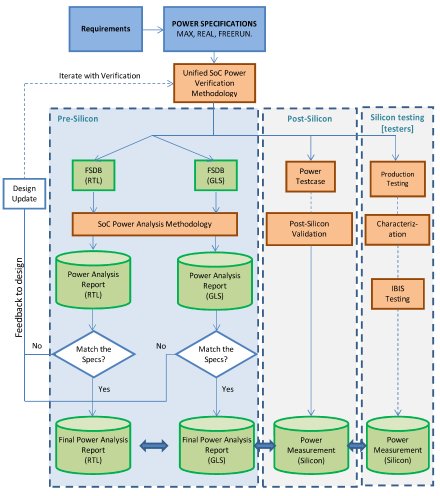
Figure 1. Pre-Silicon Power Analysis and Post-Silicon Measurement Flow
1.1 Pre-Silicon Power Analysis
In this phase, the design team will conduct the Power Analysis of the Design. After the initial estimates based on switching activity and logic, the estimates is done at RTL stage. However using traditional flow, an accurate power assessment cannot be guaranteed until gate level netlist after timing closure is available. This can lead to deviation from the specification resulting in late design changes.
Requirement driven power estimation methodology is used for accurate power estimation at early stage of design thus providing early feedback to the architecture team as illustrated in below diagram. The Fast-Signal Database (FSDB) file is used as an input. The generation of FSDB from the SPP along with overall methodology is described in the subsequent sections.
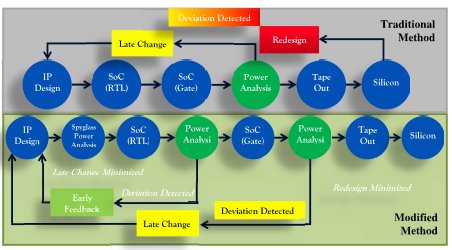
Figure 2. Traditional Flow v/s Modified Flow
The Power Architecture team uses PTPX EDA tool to generate the Power Analysis report which is used as feedback to the IP Design team. This analysis is done multiple times for RTL and Gate Level Netlist to get good correlations before the design release.
1.2 Post-Silicon Power Measurement
After the silicon arrives, the first measurement starts at the wafer level. Detailed measurements are performed by the Product Validation Team. Multiple power measurements as per defined power scenarios are done by running power pattern in the different operating modes on the packaged devices. The Characterizations team performs the selected power measurements on multiple devices selected from different technology split corners.
1.3 Correlating the Power Analysis and Power Measurement
The power numbers between Pre-Silicon and Post-Silicon are correlated at each stage to be within the bounding box as per the specification. This is quite challenging as each tool will need a different file format as the input for the analysis. Lot of iterative effort and time is spent to weed out inaccuracies in power correlation due to different test environment setup not only between pre and post silicon but also across different post silicon platforms.
The next section elaborates on the comprehensive methodology using a common framework to synergize across different platforms. This methodology is proven on silicon and has resulted in early power estimation and actual silicon measurements to be within ~6% deviation limit hence saving expensive silicon re-designs.
2 Unified SoC Power Pattern Methodology
The SPP is a collection of test codes that aims to stimulate respective modules in the SoC to generate power consumption.
The main advantage of the SPP is its code reusability, such that SPP can be re-used in many different platforms (such as Cadence NCSIM Simulation, Board, Production Tester, and Characterization Tester).
2.1 Overview
The following diagram shows the overview of the SoC Power Pattern methodology, from the development to multiple test stages where the SPP is used in respective test platform.
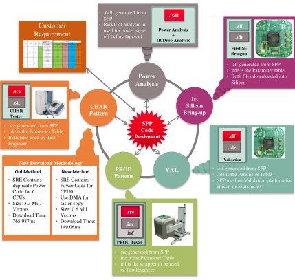
Figure 3. Unified SoC Power Pattern Methodology Diagram
As illustrated in Figure 4, the Unified Methodology consists of several stages that can be summarized in the following order:
- Customer Requirement Preparation.
- SPP Code Development.
- Power Analysis.
- 1st Silicon Bring-up
- Validation
- Production Tester
- Characterization Tester
2.1.1 Customer Requirement Preparation
The requirements are defined by concept team which is used by architecture and other teams. In the earlier stage of the development of the SPP, the Power Concept Team will align directly with the customer to capture the requirement for each Power Scenarios. We can consider following four main Power Scenarios:
- MAX Power (worst case power consumption),
- REAL Power (real case scenario for customer application),
- Application Use Case Power (e.g. activating Radar Interface), and
- ED Power (activating Emulation Device)
Apart from the above list, there are also Sleep, Standby and other Power scenarios. Each of these scenarios will have its own requirements. These Power scenarios differ mainly in the SoC configuration such as :
- Number of active modules,
- Module clocks frequencies,
- Bus clocks frequencies.
2.1.2 SPP Code Development Environment
The SPP code development is one of the main activities. The focus is on creating test code which will stimulate module activities inside the chip. SPP is developed during Pre-Silicon RTL development stage. The following diagram show the various blocks of the SPP environment:
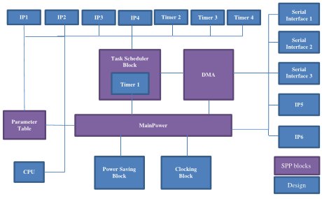
Figure 4. SoC Power Pattern Code Structure
SoC Power Pattern Code environment consists of the following main elements:
- Main Power module,
- CPU module,
- Clocking module,
- DMA module,
- Power Saving module
- IP modules
- Task Scheduler Block triggers different blocks based on concept input to create customer use case scenarios.
- Parameter table
The details of this SPP are described in following section.
2.1.2.1 Parameter table
It includes the specification details from the customer. Same parameter table is used across different platforms for consistency and maintained by central SoC Test Pattern team. Parameter table includes details on the type of the Power Scenario as shown in below diagram.
2.1.2.2 Preloading of Parameter table
The test parameters are not located in the source code, but preloaded to the defined SRAM location before the code execution. The test code flow is controlled by externally preloaded parameters. Parameter file is maintained at single/common location.
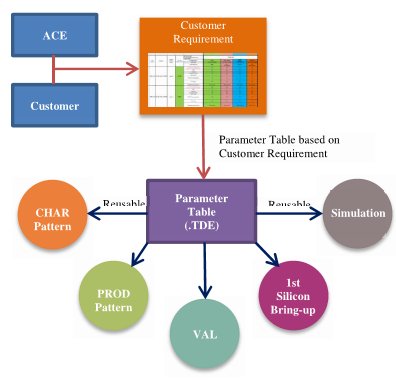
Figure 5. Reusability Diagram of Parameter Table
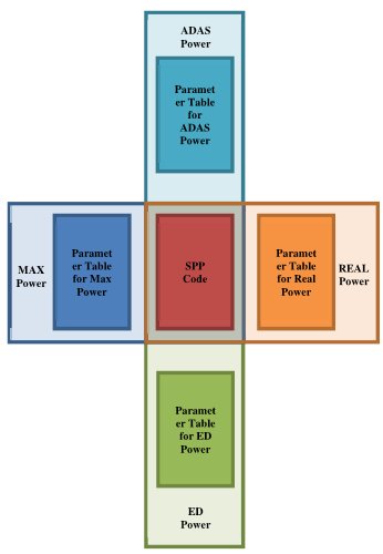
Figure 6. Portability Diagram of SPP
Upload of different parameter file is done by application reset. Some of the obvious benefits of this parameter file approach are listed below:
- Flexibility and ability to generate multiple test scenarios without deep knowledge of the source code.
- Automated approach to avoid the manual edits leading to incorrect configuration.
- Clear versioning of the parameter scripts in the source code repository
- Generate different test scenarios without any software modifications.
- Reuse across multiple platforms.
2.1.2.3 SPP Code Operation
The MainPower module is the central block of the SPP Software. This block initializes the framework based on the settings in Parameter Table. It starts with system clocks initialization followed by initialization of the modules.

Figure 7. Init () and Run () of IP Modules ,Retriggering using DMA & Task Scheduler
This step involves activation of the module clock and the respective modules without any transaction as depicted in figure 9. After the completion of initialization phase, the MainPower module triggers the respective modules to initiate data transfer in order to stimulate activities needed for the power measurement.
To get the correct power measurement, it is necessary to keep the IP Modules active. This can be achieved by retriggering the IP Modules after completion of the first run. This is when the DMA and Task Scheduler comes into picture. At the end, the postprocessing() function will check whether the IP Modules are running and/or the received data of the data transfer is correct. These checks ensure the following:
- Modules enablement matches with the configuration as per specification.
- Data transfer and interaction is as per specification
2.1.3 SoC Power Analysis
As described in earlier section SoC Power analysis starts with the RTL stage to get an early estimation of the Power Consumption of the chip.
The Fast Signal Database (FSDB) file from the SPP is delivered to the Power Analysis Team. Functional simulator identifies time frame that contains module activities.
2.1.4 First Silicon Bring-up
The same test frame work is use in silicon. It requires generation of the .ELF file from the compiled SPP code. This is downloaded with the respective Parameter Table (in the form of TDE format).
The unified test framework provides benefit of using universal ‘.ELF’ file for various Power Scenarios. The user only has to download the desired Parameter Table for selecting specific Power Scenarios (MAX, REAL, Application use case, Emulation Device). Below figure illustrates setup for first silicon bringup
The target of the 1st Silicon Bring-up is to:
- Ensure that the SPP run properly on Silicon.
- Complete initial leakage power measurement in Room and Hot Temperature.
- Complete initial overall power measurement of the chip for various Power Scenario (MAX, REAL, ADAS, ED) in Room Temperature and Hot Temperature.
2.1.5 Validation
Validation phase starts after the 1st Silicon Bring-up. Post silicon validation includes functional, robustness validation and power measurements. In this phase, more detailed power measurement of the silicon is conducted for different power modes:
- Power Measurement of each module at various temperatures.
- Power Measurement of each CPU at various temperatures.
- Measurement of leakage current at various temperatures.
The unified methodology allows usage of same setup as 1st silicon bring up for the validation stage. The same common format is used (.ELF and .TDE file).The following diagrams show the correlation between the measurement in the Validation setup and its deviation from the expected result from the customer specification.
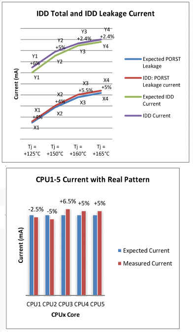
Figure 8. Leakage Current of Real Power scenario and CPUs Current Measurement with Real Power Scenario
2.1.6 Tester – Pattern
The Production Tester requires different file formats to run the SPP code. The unified methodology provides common framework to generate all these tester compliant file formats from the same SPP code. The SPP code is compiled to generate the .SRE file. Special wrapper code (.INF file) is used to download the SRE file into the tester. The Parameter Table file format here is ‘.INC’ file. Unlike Production tester, the Characterization Tester only requires SRE and the TDE file as shown in below figure
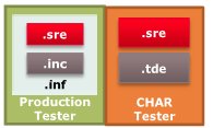
Figure 9. Files used by Production & Characterization Tester
2.1.6.1 Improvement in Download Methodology
Download of the ‘SRE’ file into the Characterization Tester can be time consuming. Limited amount of Tester Memory further adds to this complexity. To overcome this challenge simplified innovative approach is used.
- Generate CPU Power Code only for 1 CPU
- Use the DMA routine to copy the code to other CPUs memory

Figure10. Improvement of Download Methodology
This simple approach facilitates reduced SRE file size and hence significantly reduces the download time, without compromising on the functionality of the code. The old and new method file size and savings in download time, memory usage is shown in below diagram. This helps with optimal usage of tester resources. Correlation Result
In total, during the design flow, we do at least six measurements, which is during the following stage:
- Pre-Silicon – Power Analysis for RTL Design
- Pre-Silicon – Power Analysis for GLS Netlist
- Post-Silicon – 1st Silicon Bring-up Activity
- Post-Silicon – Validation Setup
- Post-Silicon –Production Test
- Post-Silicon –Characterization Test
The deviation is minimal and it is proven to be within 6%.
3. Conclusion and Benefits
In this paper we have presented Unified Methodology for Effective Power correlation and Signoff. This end to end comprehensive methodology is proven on silicon and provides following main benefits:
- Minimize late design changes/re-spins. Early and accurate estimation of SoC power and good correlation of results with silicon minimizes late design changes or design re-spins.
- Promotes reuse. Common frame work promotes reuse across pre-silicon and post silicon platforms.
- Early silicon bring-up. Easy replication of issue in pre-silicon verification environment for debug and re-generation of pattern.
- First time right. Minimize pattern re-delivery. Fully automated and Configurable flow minimizing manual error and effort for generation of test code to meet the requirements of different platforms.
4. References
[1] Clarke E. FPGAs and Structured ASICs: Low-Risk SoC for the Masses [Online]. Available: http://www.design-reuse.com
[2] V. Tiwari, S. Malik, and A. Wolfe, “Power Analysis of Embedded Software: A First Step Towards Software Power Minimization,” IEEE Trans. VLSI Systems, vol. 2, pp. 437–445, Dec. 1994.
[3] Ghodrat, M.A.; Lahiri, K.; Raghunathan, A., "Accelerating System-on-Chip Power Analysis Using Hybrid Power Estimation," Design Automation Conference, 2007. DAC '07. 44th ACM/IEEE , vol., no., pp.883,886, 4-8 June 2007
[4] S. Nithin et al., "Dynamic voltage (IR) drop analysis and design closure: Issues and challenges," in Proc. of ISQED, pp. 611-617, March 2010.
5.Glossary and Acronyms
| Acronym, Abbreviation | Description |
| ELF | Executable and Link Format |
| FSDB | Fast Signal Database |
| GLS | Gate Level Simulation |
| PORST | Power On Reset |
| RTL | Register-Transfer Level |
| SoC | System on Chip |
| SPP | SoC Power Pattern |
| TDE | Tableau Data Extracts |
| VAL | Validation |
Related Semiconductor IP
- NPU IP Core for Mobile
- NPU IP Core for Edge
- Specialized Video Processing NPU IP
- HYPERBUS™ Memory Controller
- AV1 Video Encoder IP
Related White Papers
- Methodology improves SoC power grids
- How Low Can You Go? Pushing the Limits of Transistors - Deep Low Voltage Enablement of Embedded Memories and Logic Libraries to Achieve Extreme Low Power
- Selection of FPGAs and GPUs for AI Based Applications
- An Industrial Overview of Open Standards for Embedded Vision and Inferencing
Latest White Papers
- Ramping Up Open-Source RISC-V Cores: Assessing the Energy Efficiency of Superscalar, Out-of-Order Execution
- Transition Fixes in 3nm Multi-Voltage SoC Design
- CXL Topology-Aware and Expander-Driven Prefetching: Unlocking SSD Performance
- Breaking the Memory Bandwidth Boundary. GDDR7 IP Design Challenges & Solutions
- Automating NoC Design to Tackle Rising SoC Complexity