Integration Optimized SuperSpeed USB3.0 IP from Cadence - Delivering Superior Value to the SOC Designer
Ranga Srinivasan, Cadence Design Systems
San Jose, California, USA
Abstract :
Need for Integration-Optimized IP
The Past -The SOC design of yesterday typically had a 70-80% Customer Differentiated Design elements, and 20%-30% of IP and Fabric that was reused. This model allowed third party IP vendors wearing the ‘IP Creator’ hat, to just focus on creating the component level design, while Integration of the component, into the SOC was left to be the task of the customer. This model worked really well, when the SOC had a single CPU, DSP, memory subsystem, IO, and a fabric interconnect.
The Challenges of today –Designs are moving towards a hierarchical structure, collection of individual subsystems each with a local interconnect CPU, DSP, and memory, and a global interconnect tying all these subsystems together, along with intelligent Interface IP, and multichannel memory. The pain points faced by the customer in today's world, is in obtaining and integrating enormous amount of IP, having to verify a system that comprise of SOC hardware and software, creation and validation of software, and not to mention the least, hitting schedule and budget. This design trend has created a gap between the IP that is supplied and the needs of the customer (whose primary role has thus become one of an Integrator). For every $1 spent on IP creation, there is $2 worth of Integration that is required to be spent to deliver fully qualified subsystems.
The Solution -The Cadence Open Integration Platform, bridges this gap, and delivers the value to the SOC Designer, through unique resources and competencies, and a team of Open IP Partners. Table 1 captures the Gap in the IP Integration, addressed by the Cadence Solution.
Table1 : Integration Optimized USB IP Value
| GAP In IP Value provided to the SOC Designer | How Integration Optimized IP Addresses this Gap |
| Modifying and Connecting IP into Subsystems | Configurable IP – No modifications needed, complete connected subsystems, and then platforms |
| Setup in Customer Tool Environment | Integrated and Optimized into Flows. Use of Software as a Service Model |
| Creating and Validating Software | Configured Drivers Running in a verification Environment |
| Verification setup and creating the SOC-wide verification environment | VIP Connected and verification environment running out of the box, including software drivers |
| Packaging, Board Design, & Validation | Reference Package and Board Kits, Integrated with Allegro |
| Floor Planning and Backend Implementation | IP Physically configured integrated into backend tools, scripts, and early floor-planning tools |
| Silicon Validation | Features, Tools, and Service for Silicon Analysis |
SuperSpeed USB3.0 IP – Demonstrating value of Integration-Optimization.
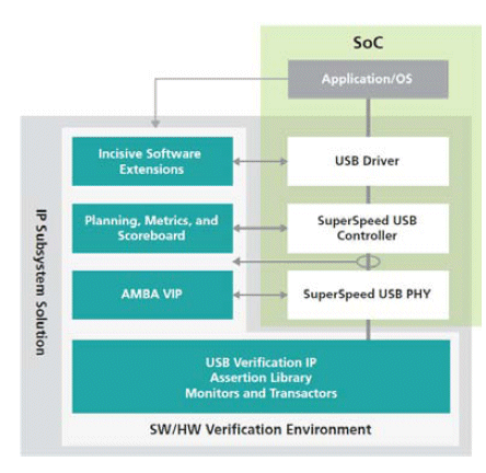
The reason we picked USB3.0, is that it is an emerging protocol, with lots of volume applications that would require high quality IP. The pain points faced by the SOC designer is further accentuated by the ramp up time needed for a newer protocol, driver layers, hardware, and software hooks needed to meet higher performance demands of the application. The Cadence solution addresses those needs by delivering a higher quality IP, a complete stack that includes, Hardware, Verification, and Software components, and as a bonus, optimized for Cadence Tool Flows. Key components of the architecture are captured in Figure 1.

Figure 1 – Integration Optimized Superspeed USB3.0 stack
The technical description that make the component of the stack as follows.
Host Controller – Compliant with Spec revision 1.0 from USBIF, and xHCI version 0.97. The optional xHCI Engine reduces software overhead, and accelerates data movement. Internal datapath width is configurable, and the core clock frequencies can be set at 125 MHz, 250 MHz, and 500 MHz values to ensure that the implementation frequencies meet the target specification.
Device Controller - Supports Control, Bulk (including Bulk Streaming), Interrupt and Isochronous Transfers. The devices controller IP comes with an optional DMA for high performance data transfer. Advanced low power is realized through features such as multiple levels of clock gating, low power states, and multiple power wells.
Serdes – The PHY is optimized for mobile applications, at 65nmLP process at 1.2V power supplies. The design implements advanced DSP for receive equalization, and pre-emphasis for Transmit control. Testability is enabled through built-in eye monitor support. The design supports both flip chip and wirebond package options, to give cost saving options to the SOC designer.
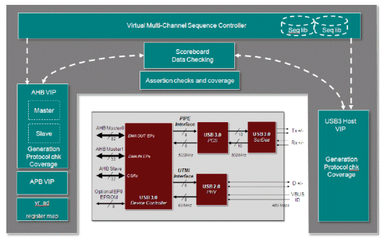
VIP – The verification IP is built with System Verilog and e language testbench. It also conforms with industry standard Open Verification Methodology (OVM), including assertion libraries, bus monitors, and transactors for creating a transaction level verification environment at the SOC level. Also included is a scoreboard, and a compliance management system (CMS).
Software Driver – The Software Driver supports simultaneous USB 2.0 and USB 3.0 operation, with advanced loopback for test and performance evaluation. It has Built in support for many embedded device classes, Low power is enabled through Link power management and selective suspend features. Advanced Quality of Service is enabled through Stream support, Command Queuing and out of order command execution. The Driver automatically generates USB descriptors, including composite devices. Advanced higher layer function classes include Feature for Mass Storage, Human Interface Devices, Wired and Wireless modems.
USB3.0 IP – Key enabler to connected subsystems and platforms
Key value provided to the IP Integrator is delivering a fully configured IP solution that runs out of the box, in a fully tested environment. A set of sample configuration options is included in Table 2. Parameters such as Buffer sizes, and Packet sizes give the configuration knobs needed to tune the IP for performance, and Quality of Service metrics. Parameters such as Interfaces, and Alternate Interfaces, provide seamless hooks into descriptor control, in the Software Driver. The USB2 PHY interface gives low power options to the designer through support for UTMI (Universal Transceiver Macro Interface), or ULPI (Universal Low Power Interface). The CoreClock, and PIPE Clock relationship gives the user integration flexibility. The PIPE Interface size parameter could be set to 8, 16, or 32 (and this corresponds to PIPE clock frequencies being configured to 125MHz, 250MHz, or 500MHz), and this certainly gives the user flexibility needed to tune the IP to meet his synthesis and post P&R timing convergence
Table2 : Configuration Parameters for USB IP
| Device Controller Configuration parameters | Host Controller Configuration Parameters |
| Inclusion of USB2 Controller | Inclusion of USB3 Host Controller |
| Number of Endpoints and type | Inclusion of xHCI Host Controller |
| Inclusion of Application Layer (AHB) | USB2 PHY Interface |
| Buffer sizes for IN and OUT Endpoints | USB3 PIPE Interface size |
| Maximum Packet Size | Number of Logical Ports Support |
| Number of Configurations | Number of Slots Supported |
| Number of Interfaces | Number of Interrupt Support |
| Number of Alternate interfaces | Support for negotiate bandwidth command |
| Exclusion of EndPoint0 | Interface Support when xHCI Controller is included |
| USB2 PHY Interface | Core Clock and PIPE Clock Relationship |
Delivering a completely validated Integration-Optimized stack

Figure 2 – Verification Environment for creation of Integration Optimized Stack
Low Power – A few special modes are enabled to guarantee lowest power of the implemented design. A power management state machine to manage power sequence in Controller and PHY. A CPF file captures the power intent of USB3 subsystem IP, integrated with CPF at the SoC level. Implement Power Shut Off technique in the controller using TSMC 65 LP library
Design for Testability – The PHY has a built in eye monitor that helps calibrate the design for eye tolerance and jitter. The design enables Prequalified Scan, JTAG, MBIST, at-speed Test ready, and Reference DFT implementation (Scan, JTAG, MBIST) using ET is available.
Software Integration - At the Device Driver Level, we have added many features such as reduced switching between User and Kernel Spaces, enhance DLLs for error handling, and processing of continuous user traffic. At the Application level, we added several knobs, for testing and validating throughput.
Benefits of Integration - Here is a sample of the issues that we resolved during IP Integration
- Missing library views for Cadence Flow such as Celtic and VStorm
- Layer assignment mismatch to foundry standard
- IPs from multiple vendors have layer configuration incompatibilities e.g. thick metal layer assignment
- Large physical macro size, blocking P/G connection causing IR issues
- No separation of on-Chip memories and/or synthesized flops –Routing and area issues
- Timing library missing power information
- Missing Bandgap & calibration modules in PHY macro
Results
The benefits of Integration-Optimization, is captured at three different levels - Quality, Performance, and Application Fit.
Quality – The efforts spent towards integration resulted in IP quality dropping from a few significant bugs, and lots of tools and flows compliant problems, to complete spec and Tools compliant in a matter of 8 weeks.
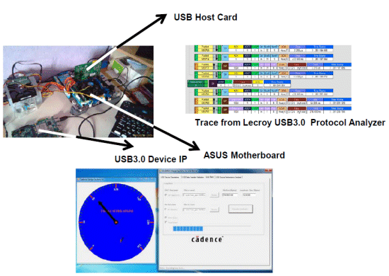
Performance - In order to demonstrate the performance, we burnt the USB3.0 Device Controller into a Stratix FPGA. The Software drivers were configured for burst read and write modes, to enable File Transfer application. The quality of the USB cable is critical to achieving at speed results in a production environment, and our IP has lots of tolerance built into it for jitter and eye opening to handle consumer grade cables. We used this setup to move large files of the order 100GByte in size, and consistently able to achieve 260MBytes/second read and write speeds
Integration - We have demonstrated Application fit at multiple levels of abstraction. We started with a set of component IPs that is configurable, connected the components together, and tuned it for high performance, and low power, and enabled it to be seamlessly integrated into a single Cadence CAD Environment. Now that is a great example of a total Solution!

Summary
The key challenge facing IP Suppliers today, is the need to focus on delivering a total solution that is more than just components tied to one another, and relieve the pain points of the Integrator. Cadence has taken on the challenge, by assembling a team of experienced professionals that can deliver on this challenge. The SuperSpeed USB3.0 protocol stack is the first of many protocols that is part of the Cadence Roadmap for the year 2010 and beyond.
About the Author
Ranga Srinivasan is Director of Product Management for Semiconductor Design IP program at Cadence. He has over 18 years of Marketing Management, and Technical Leadership experiences in the area of Systems-On-Chip for High Speed Interfaces, Embedded CPUs, Wired and Wireless networking. He has held leadership positions at companies such as Intel Corp, Marvell Semiconductor, and startup companies such as Tensilica, Nishan Systems, IntellaSys, and MoSys. He has a Masters Degree in Computer Engineering from University of Cincinnati, and Bachelors Degree in Electrical Engineering from Indian Institute of Technology, Madras.
Related Semiconductor IP
- SuperSpeed USB 3.0 Host Controller Supporting SSIC and HSIC
- SuperSpeed USB 3.0 Dual Role Device Controller, Configurable for SSIC and HSIC
- SuperSpeed USB 3.0 Device Controller Supporting SSIC and HSIC
- SuperSpeed USB 3.1 Host Controller Multiport
- SuperSpeed USB 3.1 Host Controller
Related White Papers
- SuperSpeed USB 3.0: Ubiquitous Interconnect for Next Generation Consumer Applications
- USB3.0 application building using low performance 8-bit microcontroller
- Scalable Architectures for Analog IP on Advanced Process Nodes
- Plug-n-play UVM Environment for Verification of Interrupts in an IP
Latest White Papers
- Ramping Up Open-Source RISC-V Cores: Assessing the Energy Efficiency of Superscalar, Out-of-Order Execution
- Transition Fixes in 3nm Multi-Voltage SoC Design
- CXL Topology-Aware and Expander-Driven Prefetching: Unlocking SSD Performance
- Breaking the Memory Bandwidth Boundary. GDDR7 IP Design Challenges & Solutions
- Automating NoC Design to Tackle Rising SoC Complexity