STBus complex interconnect design and verification for a HDTV SoC
Micro-architecture and performances modeling group – Home Video Division STMicroelectronics- Grenoble
1 HDTV Soc Overview
To support High Definition Television (HDTV) application, the System on Chip (SoC) presented in this paper has to support multiple and concurrent internal processes. Most of these operations read data from memory, process them and store the resulting data into memory. Each functional unit of the system is responsible for a specific data processing, but all the data are stored in the same shared external memories. Many processes are running concurrently. The architecture and performance of the internal bus is therefore essential to the SoC functionality and performance.
Dedicated for dual HDTV market, the 65 nm chip recently developed by STMicroelectronics integrates one host CPU, two video decoders enabling the decoding of MPEG-2, H264 and VC1 video frames, dedicated micro-processors for audio decoding and many peripherals for internal or external exchanges.
All data transfers are routed on an internal interconnect bus, based on STBus protocol. Interconnect is in charge of data transfer from master (called initiator) to slave (called target) components.
This paper describes shortly the STBus protocol retained for implementation of the SoC interconnect. The bus is designed with the STBusGenKit internal tool for automated generation of the interconnect. This kind of tool is a precious help given the complexity and the number of parameters to set in such a modern SoC interconnect.
The results are then presented with the description of the bus parameters definition setting guidelines and global concepts which drive the bus architecture.
The last part will introduce the functional verification platform based on random and directed tests, including automatic STBus protocol checkers.
2 STBus presentation
2.1 Overview
The STBus protocol defines a set of communication methods and interface boundaries which ensure that STBus-compliant IP may be reused across multiple projects and design groups.
Modules using these interfaces communicate using a pre-defined set of communication primitives or transactions which are then mapped onto a standard interface. The functional requirements of the transfer are defined by the operation, whilst the performance and protocol of the communication is defined by the interface (of which there are several types defined).
The figure below details all the signals possibly used in a STBus interface.
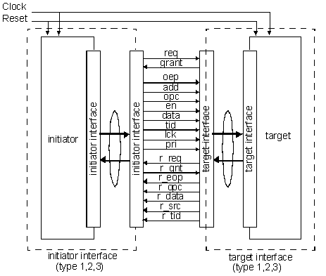
A typical module will have a number of signals corresponding to interface defined by STBus protocol. It would generally need only a subset of the possible available operations to be mapped onto a defined interface subset as appropriate for its requirements.
The interface subset used depends on the module’s requirements, port type (initiator or target), preferred data width (8, 16, 32, 64, 128 or 256 bits) and whether it requires more advanced features.
At the lowest or peripheral level, the STBus corresponds to a simple handshaking interface, whilst the more advanced definitions include efficient support for a pipelined, split phase communication media which is able to take advantage of concurrency between multiple modules.
2.2 STBus Types
Three types of transfer are defined in the STBus protocol:
2.2.1 Type 1: Peripheral
This is the simplest interface and supports a subset of the full transaction set. It is targeted at small low data rate modules which have only requirements for configuration register programming or controlled data transfer.
Each request packet has a corresponding response packet of the same length and in the same order. Operation requests are repeated in each cell.
2.2.2 Type 2: Basic
This adds support for split transactions to the peripheral interface. To simplify module design, all request/response packets are symmetrical and ordering of all operation sequences is enforced.
2.2.3 Type 3: Advanced
This extends the basic to a full split transaction packet implementation with asymmetric request/response packets and full error support. It also allows the system to relax request/response ordering properties to allow modules to take advantage of system concurrency.
In order to increase bus efficiency, initiators may request an operation only once, at the start of a packet, and then send several other cells of data in the same packet, receiving back a response packet of a different length.
2.3 STBus Transaction
2.3.1 Cells, packet, message
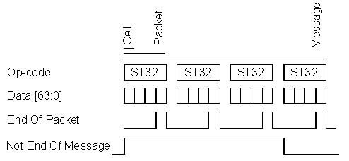
At the lowest level of any STBus transaction the “cell†is the most basic data information that can be transferred along the bus within a single clock cycle; its size equals that of the data bus.
Cells can be grouped together into “packetâ€; the last cell is characterized by the end of packet signal (EOP) high.
The “message†is a set of packets, ending with a packet having the “not end of message signal (tid<4>) low.
2.3.2 STBus op-code
Each transaction is defined by a suit of operation codes (op-code) which fixes the type of access (read, write, read modify write, swap, flush and purge) and the number of byte (1, 2, 4, 8, 16, 32, 64,128).
The chronogram bellow shows an example of four store 32 bytes message; split into four packets of four cells each, according to a 64 bit width bus.
Arbitration is a process by which it is decided which initiator can take possession of the system resources, depending on its priority and the implemented (or selected) arbitration scheme.
3. Automated STBus generation: STBusGenKit and Block Assembler
3.1. Overview
STBusGenKit is an internal tool of STMicroelectronics developed to help STBus interconnect design.
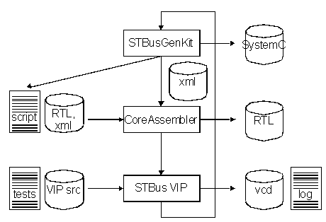
It provides a library of STBus components which can be instantiated, customized and connected through a graphical user interface. Initiator and target models can be integrated to generate a complete platform in SystemC language. For design flow a RTL netlist is generated by the Block Assembler tool, using scripts delivered by STBusGenKit.
The figure below summarizes design flow with tools, input files and results.
3.2. Component
STBusGenKit functional components are:
3.2.1. Node
This component is responsible for traffic arbitration and signal propagation across the bus from initiators to targets (request packets) and from targets to initiators (response packets). It can support different arbitration schemes defined during interconnect generation. These schemes include static or dynamic priority, least-recently used and latency-based algorithm.
Its structure has three possible topologies:
-
Shared Bus: only one target is accessible at any time.
-
Full Crossbar: many initiators can access separately different targets at the same time.
-
Partial Crossbar: a mix of both previous topologies.
For specific traffic generators bandwidth limiters can be used to guarantee that peaks of traffic occasionally generated by some initiators (typically CPUs) will not starve other initiators.
The filter feature of node avoids any access to any target if there is already a pending access to another target. This prevent “out-of-order†issues. It is mandatory in front of initiators that do not support “out of order†response typically initiators that conform to the STBus type 2 protocol.
3.2.2. Register decoder
This is a node with only type 1 address decoding feature (see configuration register decoding).
3.2.3. Frequency /type/size converter
Grouped under a single “generic converter†instance this block covers three types of conversions: frequency, type and size.
The frequency converter allows to exchange transactions across two clock domains to exchange. It can consider the two clocks as synchronous, semi-synchronous or asynchronous. However in practice, even though some clocks of the Soc are synchronous, only asynchronous architecture is used. This simplifies clock tree implementation.
The type converter transforms one type of STBus protocol in another one. It is mainly used at interconnect initiator side to be able to arbitrate together type 2 and type 3 plugs. At the opposite side type 1 and type 2 targets must be accessible by type 3 traffic.
The size converter performs data width up or down sizing (for example to convert packets of 64 bit cells into packets of 128 bit cells). Like type frequency and type converters it is needed to regroup together many sources of traffic.
Usage of generic converter is useful to connect two clusters of different size, type and frequency while keeping an efficient traffic shape.
3.2.4. Buffer
This component introduces a re-timing stage in order to met timing constraint.
It is also mandatory between two consecutive nodes.
3.3. Methodology
The RTL generation flow is split in several stages:
-
Global interconnect and configuration register decoding capture in STBusGenkit (graphical tool),
-
Add initiator and target models for system C performance verification platform (see later),
-
Automatic or manual parameters setting to differentiate each initiator traffic (source information),
-
Automatic check of all STBus parameters,
-
Automatic launch of Block Assembler,
-
RTL generation with integration of non STBusGenKit components (detailed later).
3.4. Block Assembler
The Block Assembler tool generates RTL code after assembly of all components using scripts generated by STBusGenkit.
Integration of non STBusGenKit components like bus analyzer for traffic measurement requires the integration of dedicated code. A specific view of these components for tool compatibility is created to automatically recognize and connect clock, reset and STBus interfaces.
3.5. Memory map
The memory map of the system is organized to minimize the address decoding complexity in the node address decoders of node and in the register decoders.
Also memory aliasing is introduced to prevent the system to stall when wrong (not allowed) addresses are generated by the initiators.
This first memory map specification is mainly driven by functional constraints of address decoding optimization and memory aliasing. A second pass of memory mapping specification is directed by physical constraints as described later, but decoding optimization and memory aliasing requirements remain needful.
4 SoC STBus interconnect
4.1 Overview
In term of implementation the STBus interconnect is split into two hierarchical levels: the “global interconnect†and the “configuration registers decodingâ€.
The “Global interconnect†arbitrates all initiators to all targets, including a intermediate target plug, which is connected to the “configuration register decoding†where STBus type 1 target plugs for IP register access are mapped.
The SoC STBus interconnect architecture is a compromise between performance on one side and implementation on the other side.
According to the application to be supported, the bus specifications have some fixed requirements such as number, type, frequency (clock domain) for initiators and targets.
Arbitration schemes, frequency conversion and internal re-timing stage should be designed to guarantee maximum bandwidth to DDR interfaces, but also taking into account the limitations of the physical implementation.
4.2 Global interconnect
4.2.1 Overview
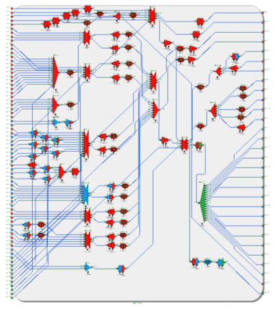
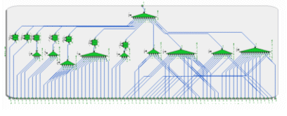
The following figure shows the STBusGenkit graphical page of global interconnect.
4.2.2 Target
The two main targets are two Local Memory Interface (LMI) ports which are responsible for transferring the data to external DDR memory devices. Each controller is able to manage two types of queue: one queue for short access with low latency (typically CPU accesses to memory), and one queue for longer transfers with lower latency sensitivity.
The STBus interconnect provides also target plugs to access an external SRAM-like interface and also target plugs for internal configuration registers.
4.2.3 Initiator
STBus initiators are split into several groups, corresponding to the different default priority level for target accesses.
CPU node
The highest priority node groups all the CPU cores.
To limit the cache miss penalty on the CPU performances, these initiators use the low-latency queue to access the external DDRs. Their traffic being very dependant of the application, bus bandwidth limiters are used.
This node can also access all others targets of the interconnect through a third target port; this will especially allow main CPU to access configuration registers.
All others initiators will be split into six groups with decreasing default priority.
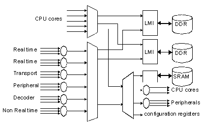
The group with the highest priority includes the video display pipelined engines. These display engines provide decoded video frames to the video composition unit at application pixel rate defined by video standards (Standard Definition, High Definition standard).
They are considered as “hard real time†processes.
In parallel with video frames, multiple graphic planes may be read from memory (DDR) to be mixed in real time with video in composition block.
The video composition result is provided to the SoC video interfaces (Video DACs, HDMI interface…) and may be written in external memory for further processing like Picture in Picture (PIP) or time shifting display.
Transport (plug 3)
This group gathers all blocks dealing with compressed data input and output. The transport stream is a typical example of compressed data coming from satellite or terrestrial or cable decoder.
Up to six input streams are filtered according to their Partial ID (PID) tags, local time stamped and saved into external memory to be read back for decryption and decoding by the two Programmable Transport Interfaces (PTI).
Up to four output streams may be fetched out of the chip from external memory through Transport Stream Generator (TSG). This functionality is required for external transcoding support (for example, H264 format can be transcoded into MPEG2 format to store HD frames on some versions of digital video disc).
Peripheral (plug 4)
This node arbitrates on-chip peripherals capable of Direct Memory Access (DMA) like Serial ATA (SATA), USB controller or Ethernet controller.
They interface external peripherals like Hard Disc Drive, Blue Ray Disc or High Definition-DVD front-end devices, digital camera, PC, portable video player…
Their position in the priority hierarchy is defined according to the data bite rate they have to support in a given application. The bit rate can also be defined by standards (Ethernet for instance). Nevertheless, they will run in “best effort†mode, since their performance may be limited by the amount of traffic in the system.
Decoder (plug 5)
Video decoding is based on two CPU cores and their hardware assists to support two concurrent High Definition H264 video decoding.
The video decoding as it is memory-to-memory process is not considered as real time but should nevertheless sustain one frame decoding within a one frame period.
In most of application scenarios, this low priority given by the default configuration is enough.
Pre-composition and non-real time memory transfers (Plug 6)
Graphical planes may be composed ahead of their presentation by using a memory to memory hardware engine. This process is of course considered as the lowest priority-holder.
The Flexible Direct Memory Access (FDMA) controllers which send and get their data to and from external memories are part of this group. This avoids to add an extra plug, which would increase needlessly interconnect complexity.
If for specific scenario it is necessary to change the default priority ordering as defined above, this is possible thanks to programmable arbitration schemes introduced in some of the STBus nodes.
4.3 Configuration register decoding
This second part of the STBus interconnect provides configuration register decoding to all others blocks of SoC.
A first architecture will only consider address split to limit register decoder complexity.
A second one will be designed to fit floor-plan requirement as will be explained further on.
This sub-interconnect uses only Type 1 protocol and register decoding blocks, but multiple clock domains are necessary to support all Intellectual Property (IP) block registers.
4.4 Clock domains
The STBus interconnect supports multiple clock domains. All clocks are considered as fully asynchronous, even if there is an integer ratio between some of them.
In the Soc considered in this paper there are 17 clocks at top of the interconnect required by application performances but also directed by floor-planning constraints. During the design of STBus interconnect some clock are split into several ones to ease timing convergence by not balancing clock onto two independent clock domains. The main impact except STBus architecture and re-design is on clock generation block.
Conversely, some clock domains are merged together to limit the number of different clocks in one physical partition. Of course this may have an impact on IP timing analysis signoff, since it may require to do the IP signoff at higher frequency. This can also bring some application restriction by reducing IP frequency. It also may introduce clock balancing between two clock trees not required by functionality.
4.5 STBusGenkit component parameters
Each STBus component has a number of parameters to be set according to type of traffic it handles.
4.5.1 Node
The STBus node is the key IP of a STBus interconnect system. It is in fact responsible for performing the arbitration among the requests issued by the initiators of the system, and among the response requests issued by the targets of the system, and for the routing of the information between initiators targets in both directions (requests and responses).
Arbitration can occur at packet or message level. The choice is defined by IP’s traffic characteristics.
4.5.2 Generic converter
Transmit and response FIFOs (packet and cell) are sized according to the input and output traffics supported by the converter.
“Store and forward†option may group many different packets of a message and send them in a contiguous transaction. Removing hole or bubble in the transfer improves DDR efficiency, which is one of the most critical parameter of SoC.
The “outstanding†parameter defines the number of request transactions an initiator may issue without having received the corresponding responses. The FIFO size of this parameter is determined by the initiators and targets characteristics. Undersizing its size may limit IP performances.
4.5.3 Floorplan constraints
After “split partitionâ€, a place and route trial is done to group internal IPs into physical partitions taking into account padring, area and timing constraints. STBus global interconnect is re-arranged internally. Mainly, initiator plugs are distributed to take into account clock domains and node partionning.
Configuration register decoding is also redesigned after “split partition†stage, in order to reduce the number of busses crossing over two physical partitions. Each physical partition finally integrates only one register decoding node per clock domain.
As nodes are purely combinatorial, physical implementation needs to introduce extra buffers to achieve timing convergence for busses crossing over two partitions.
5 Verification platform
5.1 Presentation
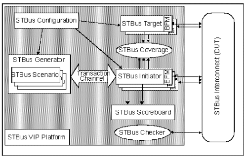
Based on Reference Verification Methodology (RVM) classes, which greatly simplify the development of Verification IPs (VIP), the STBus VIP platform is automatically generated in Block Assembler environment through dedicated plug-ins. They deliver memory mapping description, list of all initiators and targets, internal register banks.
The STBus VIP supports all types of STBus protocol. The VIP platform consists of these components:
-
STBus Configuration: it includes system parameter (number of initiator/target, routing map, internal register file…) and IP configuration (initiator/target type, protocol type, bus size, optional signals, specific behavior…).
-
STBus Transaction: set of classes according to the different layers of the STBus protocol (cell, packet, message…) with constrainable data (operation code, address, stored data, length of scenario, latencies…).
-
STBus transaction Channel: FIFO element of in charge of holding a list STBus Transaction objects.
-
STBus Generator: it is in charge of generating STBus Transaction scenarios pushed into STBus transaction Channel.
-
STBus Initiator: gets STBus Transactions from its STBus Generator, through the STBus Transaction Channel. Drives the bus and grants responses.
-
STBus Target: grants requests, gets response cells into response cell channel and behaves as a memory or random target.
-
STBus Monitor: gets request from the bus, checks address and operation code, buffers request, gets responses cells from the bus, send cells to functional coverage module and to scoreboard for routing and data integrity checks.
-
STBus Scoreboard: performs self-checking on transaction.
-
STBus Coverage: keeps trace of all transactions data and routing, scenario type and request and grant latency. May provide bandwidth information.
-
STBus Checker: checks STBus protocol validity, written in System Verilog Assertion (SVA) language.
5.2 Limitations and constraints in STBus protocol verification
One issue that appears when using the VIP platform liked to the hypothesis used at interconnect level regarding STBus protocol. For example, some IP initiators are supposed to exchange only with one target at a time. This avoids integration of filter in STBusGenKit node which is able to re-order traffic from different targets. But the generation of random tests should take this fact into account, otherwise test will fail.
Spared plugs (introduced for future enhancement) have to be declared as non-standard STBus target manually. They are connected to custom target block in Block Assembler netlist, which always provide error response operation code. This model is declared and checked by the STBus VIP platform.
Being able to introduce specific rules for each model of initiator is a key for such customized development.
5.3 Tests random and directed
Two types of tests have been developed to stimulate the VIP platform and perform functional verification.
The first set of tests generate random traffic from STBus initiators. The purpose of these tests is to verify separately the connections between each initiator and all the targets it should be able to access. To cross-check memory mapping of configuration register decoding, transactions are sent to first, last and random addresses of all targets.
During these tests all possible types of traffic (operation code, sources, message…) supported by the STBus initiator must be generated.
In enhanced tests many or all initiators send competitive request to check arbitration schemes in default configuration with different latencies from IPs to introduce possible out of ordered response traffic. Full or partial cross-bar capability, arbitration level (packet or message) and filter effect verifications are part of these tests.
Some other tests are more directed like sending requests from many competitive initiators request to check arbitration schemes after node’s priority register re-programming.
Bandwidth limiters of CPU’s node are tested in the same conditions with two sets of priority for each port: one high level during a fixed period, one low level outside.
Others patterns are linked to security, testability and validation features; they are all developed on the same principle of directed tests.
5.4 Results
The STBus VIP platform provides log files with many possible levels of transaction details.
5.5 Others possible tasks at SoC or IP level
The STBus VIP platform could also be used at SoC level to generate random traffic for top level functional verification tests, or during IP development to check initiator STBus protocol integrity or simulate target model.
6 Performance verification
A performance verification platform is developed, which uses the interconnect System-C model provided by STBusGenkit tool. The platform includes also traffic generators to model the STBus traffic for a given application scenario. They are specific to the scenario under study.
The purpose of this platform is to check that the performance requirements for each class of IPs are met (real-time, bandwidth and latency constraints).
This verification process allows to confirm that the interconnect arbitration scheme and FIFO sizing are correct.
7 Conclusion
As described in this paper, the design and verification of Soc interconnect require several actions managed by dedicated tools. In spite of its complexity, the flow should be able to support architecture modifications or improvements with acceptable planning impact.
The limited number of STBusGenKit components and their great flexibility provide refine possibilities, even late in the design implementation schedule.
But STBus protocol has some limitations in terms of performance, scalability, power consumption and reliability.
For future developments, Network on-Chip like STNoc protocol will be introduced. Based on a flexible packet-based communication, micro-network infrastrures are developed to provide more and more data exchange capabilities.
Reference documents: VIP STBus User Guide by Francoise Casaubieilh (Synopsys Verification Group)
STBus Asynchronous Decoupler: an answer to the IP integration issues in future technologies by Alberto Scandurra & Salvatore Pisasale from STMicroelectronics (Italy) & Daniele Mangano from University of Messina (Italy)
An Application-Specific Design Methodology for STbus Crossbar Generation by Srinivasan Murali, Giovanni De Micheli
Computer Systems Lab Stanford University
Stanford, California 94305
See also:
http://www.st.com/stonline/products/technologies/soc/stbus.htm
Related Semiconductor IP
- NPU IP Core for Mobile
- NPU IP Core for Edge
- Specialized Video Processing NPU IP
- HYPERBUS™ Memory Controller
- AV1 Video Encoder IP
Related White Papers
- Integrating VESA DSC and MIPI DSI in a System-on-Chip (SoC): Addressing Design Challenges and Leveraging Arasan IP Portfolio
- A RISC-V Multicore and GPU SoC Platform with a Qualifiable Software Stack for Safety Critical Systems
- Design and implementation of a hardened cryptographic coprocessor for a RISC-V 128-bit core
- Bigger Chips, More IPs, and Mounting Challenges in Addressing the Growing Complexity of SoC Design
Latest White Papers
- Ramping Up Open-Source RISC-V Cores: Assessing the Energy Efficiency of Superscalar, Out-of-Order Execution
- Transition Fixes in 3nm Multi-Voltage SoC Design
- CXL Topology-Aware and Expander-Driven Prefetching: Unlocking SSD Performance
- Breaking the Memory Bandwidth Boundary. GDDR7 IP Design Challenges & Solutions
- Automating NoC Design to Tackle Rising SoC Complexity