SoC Integration of Programmable cores
Andreas Hoffmann, Olaf Zerres, Achim Nohl : CoWare Inc., San Jose, USA
Abstract :
Current and future SoC designs will contain an increasing number of programmable units to meet flexibility, performance and cost constraints. Only when integrating processor IP blocks into the SoC system model as early as possible, architectural alternatives can be evaluated effectively. Furthermore, the embedded SW can best be developed, debugged and profiled when simulating it in system context.
CoWare provides a comprehensive system level SoC design environment which supports the designer in creating processor IP blocks as well as in using them to design and program optimal SoC platforms.
1. Problem Statement
The emerging platform based design paradigm poses enormous challenges to conceptualize, implement, verify and program today’s complex SoC designs. System architects are obliged to employ heterogeneous computational fabrics to meet conflicting requirements with respect to performance, flexibility and power efficiency. The complexity problem of increased heterogeneity also applies for the on-chip communication: numerous busses of different types are necessary to cope with the escalating data traffic [1].
In the predominant industrial praxis, design of complex and programmable SoCs still follows the traditional flow, where the textual architecture specification phase is followed by sequential and mostly decoupled implementation of HW and SW parts. Finally processors, busses, memories and dedicated logic blocks are integrated on the HDL based implementation level. The high complexity and poor simulation speed on this level prohibits consideration of architectural tradeoffs and integration of the embedded SW has to wait even until the silicon is available.
Due to the lack of early system integration, complex SoC are either over-designed or fail to fulfill the performance specification. Especially the performance related to the SW part, like e.g. CPU load, impact of the RTOS, or SW response time, can hardly be analyzed without a cycle accurate simulation model. Furthermore the SW performance is heavily affected by the communication and memory architecture, so an isolated consideration of a single processor may hide potential bottlenecks due to bus utilization and memory access latency. This kind of issues has to be addressed as early in the design flow as possible to prevent from late and costly changes of the architecture specification.
In this article, we first introduce the underlying technology for system level design and smooth integration of processor IP into the system context. Then we highlight further design steps at the platform level: multiprocessor debugging and performance analysis. Finally, a case study of a complex dual processor JPEG image processing system is presented.
2. System Level Design
Today any embedded processor is just a component in a complete system, which may include further programmable processors, accelerators, and I/O blocks as well as a heterogeneous communication architecture. System-level simulation is required in order to verify correctness and performance of the entire hardware/software system.
In this context, SystemC [2] is considered as the emerging industry standard for system architecture design, because on the one hand side being a native C++ library it fits well into any SW flow. On the other hand side, SystemC incorporates mandatory HW semantics like concurrency, module hierarchy, and explicit timing to create architectural models.
However, having an expressive language alone is not sufficient to enable system-level design, instead the major bottleneck in terms of simulation speed and modeling efficiency is caused by the highly detailed Register-Transfer Level (RTL) modeling style. Therefore, SystemC 2.0 advocates the Transaction-Level Modeling (TLM) paradigm [3], where the pin-accurate communication between modules is replaced by condensed Interface Method Calls (IMC). Especially for complex bus protocols like AMBA AHB, this simplification attains up to two orders in simulation efficiency [4] without sacrificing cycle accuracy. TLM along with the concept of dynamic sensitivity also results in a very condensed modeling style, which is essential to motivate the creation and maintenance of a separate model for architectural exploration at the system level.
3. CoWare’s Solution
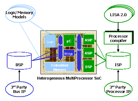
Based on the SystemC TLM paradigm, CoWare® Inc. has recently introduced the ConvergenSC™ product family, an EDA solution addressing system-level design and verification of Multi-Processor SoCs (MP-SoC). The integration of the LISATek Processor Design Suite into the CoWare N2C tools family establishes a comprehensive design and verification environment addressing all aspects of platform based design. As depicted in figure 1, the combined solution enables early IP integration, and by that profiling driven exploration and optimization of the complete SoC.

Figure 1: system level IP integration
The bus architectures as well as processor cores are basically considered as 3rd party IP reuse. The processor cores alternatively can optimally be tailored for the respective application by using the LISATek Processor Design Suite.
Transaction-Level Modeling (TLM) is the enabling technology for fast but also accurate simulation of MP-SoCs. Instead of costly modeling and simulating the complex RT-level pin-wiggling communication, the Interface Method Call (IMC) principle is applied. This allows simulation speed beyond 100kcycles/second, as well as easy and early IP integration.
The concept of dynamic sensitivity applied here does not only enable higher simulation speed, but also allows intuitive modeling and high code density. For example, the bus FSM resides inside the bus model with the connected modules being sensitive to the expected events. This is much more efficient than implementing the bus protocol FSM or parts of it in every module.
Within the large class of TLM communication, the system designer can choose between a blocking transaction API and a non-blocking transfer API for a fine-grain trade-off between modeling effort and simulation accuracy. The transaction API enables modeling inter module communication very early just by redirecting any read and write access of an instruction accurate processor simulator to the outside. The transfer API, in contrast, is tailored for cycle accurate processor models and invokes any atomic communication event explicitly in the respective processor cycle.
The LISATek bus model provides a generic set of communication primitives for blocking as well as non-blocking bus access. This generic memory interface allows any LISATek processor model to be hooked to any bus model.
After an executable virtual prototype has been created, we will now focus on the verification of the MP-SoC architecture and the embedded Software.
4. Multi-Processor Debugging
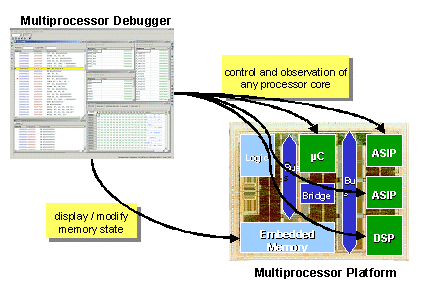
For user friendly debugging and online profiling of the embedded SW and its platform, the user always - at simulation runtime - has the possibility of getting the full SW centric view of an arbitrary SW block. All other SW blocks that are currently not considered still run at maximum speed.
To keep the potential for highest possible simulation speed in a complex SoC simulation, the data exchange between the processors and their respective SoC environment – which is always necessary independent of the user's system observation - must be highly optimized. This can only be guaranteed if all processor simulators reside within one executable on the host such that no slow Inter Process Communication (IPC) is necessary for this task. IPC is applied if and only if the user decides to observe or take control over a certain processor simulator.
The processors to focus on can be selected at simulation runtime. Thus, only one or two debugger GUIs are sufficient even to debug complex multiprocessor systems.
The remote debugger frontend instance offers all observability and controllability features for multiprocessor simulation as known from standalone processor simulation. Even resources external to a processor module but mapped into its address space like peripheral registers and external memories can be visualized and modified by the multiprocessor debugger GUI.

Figure 2: dynamic connect multiprocessor debugger
The SW developer can dynamically connect to relevant processors, set break/watch points in respective code segments, disconnect from simulation and automatically re-connect when a breakpoint is hit.
After the functional verification of the complete HW/SW platform, the next important task is the verification of the performance requirements.
5. Platform Profiling
The system architect needs to create a platform that meets the performance requirements at the lowest possible cost. Having assembled own as well as 3rd party IP for processors, SW and the communication in between, the designer needs information as detailed and accurate as possible about the system’s performance to be expected. Thus, CoWare’s analysis capabilities cover all aspects of platform profiling.
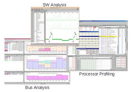
The bus analysis evaluates bandwidth requirements and can detect bottlenecks in the communication architecture. The SW analysis enables execution time profiling on application level. For example, a gantt diagram shows a detailed cycle count for every function call. The LISATek processor profiling exactly shows the utilization of the processor resources (registers, functional units) and also highlights performance critical loops in the application on assembly level, for example.

Figure 3: comprehensive profiling environment
The platform profiling information is collected during system simulation. The user always can trade simulation performance against depth of profiling by selecting only the relevant parameters, e.g. the bus utilization. The tight integration of CoWare’s bus and SW analysis with the processor simulator enables the system developer to trace which part of the application is currently executed and what bus transactions are initiated.
These powerful profiling capabilities are provided automatically for every system platform to be analyzed. The complex APIs for bus analysis and SW analysis all are generated together with the platform simulator. Also the processor simulator itself, when newly generated using the LISATek tool suite, automatically is equipped with the processor profiling capabilities. The turnaround time for modifying and re-integrating a processor is about 10 minutes. This gives an enormous productivity gain to the designer!
6. JPEG Case Study
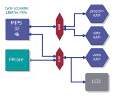
The outlined design methodology has successfully been applied to the development of a JPEG image processing system (figure 4). The system reads compressed image data from the flash memory of a digital camera and decompresses it to apply filtering algorithms and special effects to the photo. An LCD connected to the video memory displays the result.
It turns out to be reasonable to use two different processor cores for this system: A MIPS32 core for decoding the JPEG and controlling the system, as well as an ASIP called FPcore, which has optimally been tailored for performing image filtering and special effects. Both processors access the common video RAM using an AMBA bus. The MIPS is connected to a second AMBA bus for accessing its remaining memory including the flash memory.

Figure 4: image processing system
The CoWare tools allow both: First, they check the correct functionality of the complete system in every design step; and second, they can give an estimation for the overall system performance very early in the design flow.
Having the system model available, quantitative values for different architectural alternatives can be obtained quickly. In case of this exemplary architecture, the MIPS32 core executing the standard JPEG decryption software [5] decodes a 256x192 sized bitmap in about 871 million cycles. Introducing a suitable instruction cache drastically reduces this value to 81.3 million cycles. In both cases, the FPcore is permanently competing for access to the video memory via the AMBA bus to show additional objects, messages, or to start filtering the image concurrently. In the latter case, 12.4 million cycles of the overall JPEG decoding time are caused by the FPcore’s activity. What the system designer needs for optimal design decisions is a reliable estimation concerning such characteristic values as early as possible.
7. Conclusion
The platform designer absolutely needs optimal tool support during the architecture exploration and implementation phase, and for programming and verifying the complex multiprocessor SoC platforms. CoWare’s powerful tool suite meets these challenging requirements.
[1] O. Ogawa, K. Shinohara, Y. Watanabe, H. Niizuma, T. Sasaki, Y. Takai, S. Bayon de Noyer and P. Chauvet, "A Practical Approach for Bus Architecture Optimization at Transaction Level", International Conference on Design, Automation and Test in Europe (DATE), 2003
[2] Open SystemC Initiative, www.systemc.org
[3] T. Gröker, S. Liao, G. Martin, S. Swan, "System Design with SystemC", Kluwer Academic Publishers, 2002
[4] G. Braun, A. Wieferink, O. Schliebusch, R. Leupers, H. Meyr, A. Nohl ”Processor/Memory Co-Exploration on Multiple Abstraction Levels”, International Conference on Design, Automation and Test in Europe (DATE), 2003
[5] Official JPEG homepage, http://www.jpeg.org
Related Semiconductor IP
- Wi-Fi 7(be) RF Transceiver IP in TSMC 22nm
- PUF FPGA-Xilinx Premium with key wrap
- ASIL-B Ready PUF Hardware Premium with key wrap and certification support
- ASIL-B Ready PUF Hardware Base
- PUF Software Premium with key wrap and certification support
Related White Papers
- Streamlining SoC Integration With the Power of Automation
- Programmable logic/customizable CPU cores adapt hardware to apps
- Enabling Secure Integration of Multiple IP Cores in the Same FPGA
- Greater Debug of a SoC having heterogeneous ARM Core's
Latest White Papers
- Boosting RISC-V SoC performance for AI and ML applications
- e-GPU: An Open-Source and Configurable RISC-V Graphic Processing Unit for TinyAI Applications
- How to design secure SoCs, Part II: Key Management
- Seven Key Advantages of Implementing eFPGA with Soft IP vs. Hard IP
- Hardware vs. Software Implementation of Warp-Level Features in Vortex RISC-V GPU