Enabling Secure Integration of Multiple IP Cores in the Same FPGA
By Bassel Soudan, University of Sharjah Wael Adi, Braunschweig University of Technology Abdulrahman Hanoun, Technical University of Hamburg
Abstract :
In this work, we discuss a security mechanism for integrating multiple IP cores into the same FPGA-bound design, maintaining their individual security, and preventing their theft and/or over deployment. The system utilizes robust cryptographic techniques and device-specific IP descriptions to achieve the desired goals. The combined methodology and supporting hardware enable the unambiguous protection of each IP core against theft, interception, reverse engineering, and over-deployment.
Introduction
System-on-chip designers today are faced with a highly competitive global market that has tightened market windows, elevated performance requirements, and heightened functionality expectations. The underlying technology (primarily FPGAs) has progressed steadily and now offers great performance, wide range of functionality, and increased flexibility. However, with this flexibility comes added complexity. To address all of these pressures, designers are increasingly relying on the reuse of ready-made designs. Be it the reuse of in-house design or the licensing of ready-made Intellectual Property (IP) cores from IP providers.
The expansion of the market for IP cores triggers concerns with IP core providers over the protection of their rights and royalties. Currently, when an IP provider licenses out an IP core, the customer receives a net-list or HDL description to be incorporated into their design. There is nothing to prevent the customer from making use of the licensed IP core beyond the limitations of the license agreement.
From a security perspective, there are numerous attack points where the security of the system and/or licensed IPs may be compromised. The customer may over-deploy a licensed IP beyond the limits set by the license agreement with the core vendor. A core vendor – if given access – may attempt to compromise the security of another vendor’s core. The programming facility may attempt to over-deploy the entire design or specific cores beyond the limits set by the contract with the system integrator. The system may be a target for theft and/or duplication once it is deployed into the field.
SRAM based FPGAs utilize a volatile configuration memory and therefore require reconfiguration after every power interruption from an external non-volatile memory. The data link between the FPGA and the non-volatile memory represents a significant security risk. To help protect against interception and possible cloning, major FPGA device manufacturers have enabled the encryption of the design data to ensure that it cannot be meaningfully intercepted between the non-volatile memory and the device [1] and [2]. While this system protects the IP from theft, it does not protect it from over-deployment by the customer or the customer’s surrogate programming facility.
There have been several proposed methods for detecting when an IPR violation occurs. Most are based on embedding hidden watermarks in the design [3] - [5]. While these methods may be successful in determining when an IPR violation has occurred, they are not useful in preventing the violation in the first place. One needs to suspect that a violation has occurred and have a clue of where it has occurred before being able to detect it. The sheer number of FPGA based designs continuously appearing on the market makes it prohibitive to even contemplate checking every single design for possible IPR violations.
In this work, we discuss a security mechanism for integrating multiple IPs into the same FPGA-bound design, maintaining their individual security, and preventing their theft and/or over deployment. To maintain the widest possible application scope, we assume the involvement of many parties in the process. We presume that a customer (system integrator) will license multiple IP cores from multiple IP vendors. These licensed IP cores will be integrated with in-house developed modules to create the overall system. We will also assume the existence of a surrogate programming facility handling the programming of the actual devices. We will also question the integrity of every participant in the process.
We will show that, at all times, the design and the individual core will be completely secure. The exchange of the cores will only be conducted in a securely encrypted form. The cores will be targeted to specific uniquely identifiable devices and cannot under any circumstances be deployed into any other devices. The only participant capable of accessing the IP core’s raw description is the IP provider. In addition, no instance of the IP core can be produced without the prior knowledge, approval, and participation of the IP provider.
Device-Specific Encryption
Our proposed licensing model enables the provider to communicate to the customer device-specific descriptions of the IP core encrypted using device-specific keys that the customer can not access. The system requires the creation of two identical copies of a common secret key at the IP provider’s site and securely on the device at the IP customer’s site. The two copies of the secret key are generated independently eliminating the need for complex key management schemes. The key creation occurs through a challenge-response mechanism based on publicly exchangeable device-specific identities.
Implementing the system requires the existence of a Device Identity Module (DIM) in each device created during manufacturing along the lines shown in Figure 1. This module will be used during an authentication sequence between the IP provider and each of the target devices that results in the generation of the pair of identical keys. It will also be the point of entry for encrypted bitstreams into the device during configuration.
In brief, two independent copies of a secret IP-vendor-specific key will be generated and stored securely inside the chip as well as at the IP vendor’s site through a simple (automatable) 4-step exchange sequence. This key will be based on random numbers generated securely within the chip (Si in the figure). Information exchanged during this key creation phase will be either publicly accessible information like device serial numbers or securely encrypted secret information that can only be decrypted by the specific IP vendor.
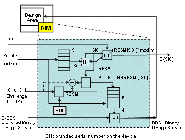
Figure 1. Proposed Device Identity Module
Exact details for the shred key creation sequence is summarized as follows:
System setup:
The device manufacturer is assumed to be trusted to implement the device identity module as specified. The manufacturer is not needed for the rest of the IP-protection protocol. For more security, the manufacturer can be involved to certify the FPGA compliance with the specification.
A trusted authority TA should certify the originality of the FPGA chips by inserting in a write only memory a secret device identity SDI as a simple certificate of origin assigned to each branded serial number SN. This can be made more secure and more sophisticated. TA publishes a verification engine which delivers a response RESM for any challenge CHv coming from outside. To avoid fraud, the trusted authority responds by adding its own additional challenge. That is, if challenged with CHv, the trusted authority responds with:
RESM = {H(CHv, SDI, CHt) | CHt} (1)
adding its own challenge CHt and sending it in clear to the verifier. Notice that the pair CHv, CHt generated by two independent random sources is unrepeatable with very high probability (if TA does not cheat). This operation is not shown in Figure 1 to simplify the presentation.
The register array S is eventually initiated by the device owner with secret content unknown to anybody following the procedures describe in [6] and [7].
Building a trusted shared secret between the device and the IP provider:
The IP customer sends the device serial number along with the purchase order for the required IP core to the IP provider i (the IP-Core will be designated as IPi from here forward).
The IP provider consults the TA server and sends a fresh self-generated challenge CHv. The server responds with a quantity as shown in (1), in addition to TA’s counter challenge CHt. The IP provider sends CHv, CHt values back to the IP customer with a fresh selected value m (product of two large primes to form a Rabin-Lock).
The IP customer applies the value received from the IP provider (CHv, CHt) to the device as a challenge and obtains its response:
C-(Si0) = {(H(RESM, Si)| RESM)}2 mod m (2)
The IP customer sends the device’s response C (Si0) back to the IP provider.
The IP provider computes the square root of the above token and gets RESM and Si0 (which is equivalent to H(RESM, Si) ). If RESM is equal to that delivered by the TA, the device authenticity is proven.
Shared Key Creation
The shared secret key Ki is then computed by the IP provider as:
Ki = H(Si0, RESM) (3)
This key is for the particular device and the particular IP provider. If an IP customer licenses multiple IP cores from the same provider to be integrated into the same design, the same key can be used to encrypt the copy of each core destined to the particular device. For every Ki in the n-entry register file K there is a corresponding entry Si in the S register file. The device thus has a capability to generate n different shared keys for n different IP providers.
For additional security, the challenges CHv, CHt could also be involved in generating Ki as indicated by the dashed lines in Figure 1. Equation (3) should then be modified correspondingly
The IP provider encrypts the IP bitstream using the key Ki to generate the ciphered bitstream C-BDS.
C-BDSi = F (IPi) Ki (4)
where F is a cipher identical to that integrated in the DIM.
The ciphered bitstream for IPi (C-BDSi) is sent to the customer. The device activated with the profile i for IPi would decrypt the bitstream with the shared secret key Ki (generated internally as shown in Figure 1) for that particular IP.
Figure 2 shows the overall 4-step exchange protocol. It is possible to reduce the number of steps if we add some procedural time constraints to the system as described in [8].
Using the encryption key of each target device, the IP provider creates a distinct encrypted copy of the IP description per device. The encrypted IP descriptions are communicated to the customer who downloads each encrypted copy of the IP into the appropriately matching device. The encrypted bitstream (shown as C-BDS in the lower left corner of Figure 1) passes through the enclosed decryption engine (shown as F-1 in the figure). The bitstream is decrypted and then passes to the configuration fabric.
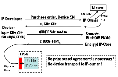
Figure 2. Secured exchange of one IP-core
Given that the encrypted IP descriptions will be decrypted on the devices themselves, then there is no possibility for the customer to cheat and create additional instances without the active participation of the IP provider. The raw IP description will never exist outside the IP provider’s control except on the device itself. The model stipulates that the design bit stream must not be extractable from the device after programming. This stipulation is easily met with modern devices that allow read-back prevention.
Application to a Multi-IP Design
To maintain the security of the IP core, the IP provider must be the only entity capable of accessing the IP’s raw description at any point of time. Not even the design software at the customer’s site is entrusted to decrypt the IP descriptions for integration into the overall design. The design software must deal with these IP cores in a black-box manner. While not revealing the internal design of the IP core, the IP provider shares compiled simulation and timing models with the IP customer [9]. These compiled models protect the details of the licensed IP but still allow the customer to perform functional simulation and timing analysis of the design. On the other hand, the physical integration of the design (including the licensed IPs) has to occur on the device itself.
The following is a description of the overall design flow for integrating multiple licensed IPs from licensing the IP’s all the way through device programming:
1. The IP providers advertise their IPs including resource requirements (number of CLBs, IOBs, BRAM, etc.) for different device types.
2. The IP customer selects the IPs to be licensed and creates a floorplan similar to what is shown in Figure 3 below. The area allocated for each IP must contain the required resources at least.
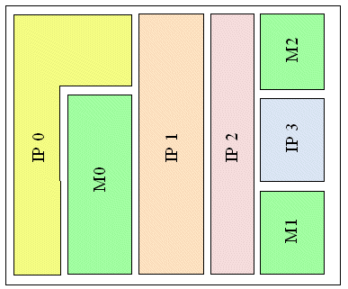
Figure 3. A design with multiple licensed IPs (IP0 – IP3) and in-house macros (M0 – M2).
Because IP core bitstreams will be individually encrypted, then the entire area of a particular core must be configured together before adjacent areas belonging to other cores can be configured. The design of modern devices such as the Virtex 4 and Virtex 5 from Xilinx is based on a tiled design [10] and [11]. The configuration array is arranged into rows that span only 16 CLBs vertically and each frame spans the vertical height of a tile [12]. This tiled design allows blocks to be of any shape with the single condition that vertically they must span multiples of 16 CLBs.
3. Upon establishing the purchase agreement with the IP providers, the customer creates a profile for each vendor on each device. This process also creates the secret keys for the IP vendors inside the devices and at the vendors’ sites.
4. The IP customer communicates to the IP provider the floorplan requirements for the licensed IP for the given device types.
5. The IP provider generates a design bitstream for the IP that meets the floorplan requirements, encrypts the design description and dispatches it to the IP customer along with compiled simulation and timing analysis models. The involvement of the IP provider is complete at this point.
6. As the aggregate bitstream is downloaded into the device and passes through the DIM module, the module will recognize the header at the beginning of each section of the stream. It will extract the location information and the profile index. Using the profile index, the DIM switches to the appropriate profile and uses the proper key to decrypt that section of the bitstream. In a manner similar to techniques used in partial reconfiguration, the decrypted configuration sequences are passed to the appropriate locations on the chip [12] and [13].
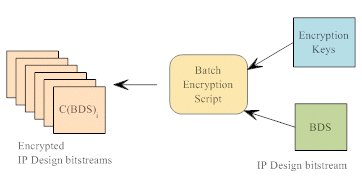
Figure 4. The IP Provider Creates Encrypted Copies of the IP Design Bitstream
7. The IP customer collects the design bitstreams for all licensed IPs from the different IP providers. Then, the customer uses “device management” software to aggregate the encrypted bitstreams of the different IPs and creates an overall bit stream to be downloaded into the device. The software prepends each section of the aggregate bitstream with a header containing the location information and an appropriate profile index understandable by the DIM module.
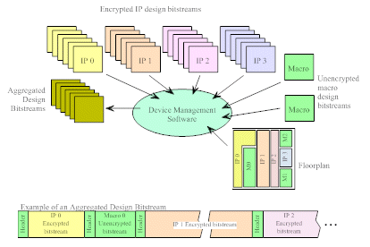
Figure 5. The Device Management Software produces aggregated bitstreams for the different devices
Because of the flexibility afforded by partial reconfiguration, the order in which the cores are integrated into the overall system is inconsequential.
Dynamic Reconfiguration
The proposed system does not preclude advanced FPGA functionality such as dynamic reconfiguration. This functionality allows off-loading of a section of the design from the FPGA device and loading a new block in its place without the need to power down and reconfigure the entire device.
Dynamic reconfiguration is constrained by the organization of the device’s configuration memory. It requires that blocks planned for reconfiguration must conform to the boundaries of the reconfiguration fabric. It requires that the replacement block must occupy the same area (or less) compared to the off-loaded block. It also requires that the interfaces of the block to the rest of the design must allow disconnecting the block’s signals from the rest of the design so that glitches occurring during the reconfiguration do not cause misbehavior in the rest of the design. Xilinx has developed a pre-synthesized bitstream called a bus macro as part of its Modular Design tool enabling partial reconfiguration in Virtex devices [13]. When inserted between adjacent blocks, a bus macro provides inter-block communication with fixed routing resources through tri-state buffers. A block on either side of the bus macro can be replaced at anytime without disturbing the block on the other side – as long as the inter-block communication remains the same.
Our proposed technique depends on partial reconfiguration for downloading the design into the device in the first place. Therefore, it is quite simple to conceive how dynamic reconfiguration would work under such a system. While adhering to the restrictions already imposed by the dynamic reconfiguration process itself, our proposed method adds a single requirement. A profile for the provider of the new IP core must have been created on the device beforehand. Following the process discussed above, the licensed core to be downloaded into the device is communicated as an encrypted description to the IP customer. During the dynamic reconfiguration process, the IP customer applies the IP provider’s profile index to the device which selects the right decryption key for the incoming block. The description is passed to the DIM where it is decrypted, and forwarded to the appropriate location on the device.
Advantages of the Proposed System
The proposed system protects the IP against over-deployment by communicating device-specific encrypted bitstreams. Short of cloning the unique SDI and the random contents of register file S, the customer (or any other party) cannot over-deploy a licensed IP. It also protects the IP against reverse engineering by denying access to the raw description or the decryption keys even for the licensing customer.
The device manufacturer’s involvement in the licensing process is not required beyond the manufacturing of devices with the DIM module. The IP providers do not need to have first hand possession – even temporarily – of the devices for key programming. The communication of the secured IP is carried out electronically and dealing with the physical devices is left to the IP customer or contract programmer. The involvement of each party is required only within their area of expertise and interest.
Limitations
A seeming limitation of the system is that only devices initialized for the combination of IPs comprising the design can be used for that specific design. While this may seem as a disadvantage, it offers the advantage of non-repudiation. The IP customer can precisely prove the IP provider’s involvement in the licensing process for each specific device. Since the IP provider ships only encrypted descriptions, and the customer-inaccessible decryption keys are created with the explicit involvement of the IP provider, it is impossible for the IP customer to have a copy of the IP that is not explicitly authorized by the IP provider. Also, it is possible to maintain a trace of the challenges and responses flowing between the IP provider and the devices as proof.
Because the IP customer must deal with the licensed IPs in a black-box manner, the ability of the customer to optimize the design of a particular core is reduced. The customer must rely on the IP provider to produce highly optimized cores. While this is a valid limitation, it is not of great concern. Because the IP provider is the one developing the core, it is highly unlikely that anyone would be able to produce better optimized descriptions of the core.
For improved security, the register files S and K in the DIM should be write-once memory. Therefore, once a device has been initialized for an IP from a specific provider, that link will be permanent. However, this limitation is not entirely intractable. First, the keys hidden in the device are IP provider specific. They may be reused for other cores licensed from the same provider later. Second, the size of provider specific data kept in the DIM (Si and Ki) is on the order of 1000 – 2000 bits. Therefore, it is economically feasible to allow a large number of profiles by adding more entries to each of the S and K register files. The numerous entries allow creation of new profiles when the chip is reconfigured for a new design containing licensed cores from different providers.
Summary and Conclusion
This work proposed a mechanism for the authenticated transfer of design information that prevents IPR violations in an FPGA design environment. The novel security technology uses combined public and secret-key cryptographic mechanisms. The resulting system offers a high level of security while still being reasonably easy to handle. The proposed mechanism allows design distribution over public networks without loss of security. The mechanisms employed are based on trustable cryptographic primitives well known in secret-key and public-key cryptography, but utilizes low complexity functions to simplify the implementation and save resources. In particular, the selected public-key technology employs squaring in a ring resulting in the simplest public key system known to date.
The system appears to be unbreakable even if the device manufacturer collaborates with the IP customer. The design transfer does not involve the manufacturer on-line and does not need the IP provider to have any contact with the FPGA devices. All transactions can run over any open communication network without prior secret sharing. The FPGA manufacturer must however be trustworthy to manufacture according to the specified hardware security architecture and not to have built backdoors in the FPGA architecture.
The system is robust and is able to accommodate designs containing multiple licensed IP cores easily. It supports advanced FPGA features such as dynamic reconfiguration and device reuse.
References
[1] Actel, “ProASIC3/E Security,” Application Note available at http://www.actel.com, cited on April 14th 2005.
[2] Peattie, M., “Use Triple DES for Ultimate Virtex-II Design Protection,” XCell Journal, Summer 2001, pp. 29 – 29, available at http://www.xilinx.com, cited on April 14th 2005.
[3] A. B. Kahng, D. Kirovski, S. Mantik, M. Potkonjak and J. L. Wong. "Copy Detection for Intellectual Property Protection of VLSI Design." Proc. IEEE/ACM Intl. Conference on Computer-Aided Design, November 1999, pp. 600 – 604.
[4] Yuan, L., Pari, P. R., and Qu, G., "Soft IP Protection: Watermarking HDL Codes," 6th Information Hiding Workshop, LNCS Vol. 3200, Springer, May 2004, pp. 224 – 238.
[5] Newbould, R. D., Carothers, J. D., Rodriguez, J. J., and HolmanW. T., “A Hierarchy Of Physical Design Watermarking Schemes For Intellectual Property Protection Of IC Designs,” Proceedings of the International Symposium on Circuits and Systems, 2002, Vol. IV, pp. 862 – 865.
[6] Adi, Wael; Soudan, Bassel; “Bio-Inspired Electronic-Mutation with genetic properties for Secured Identification”, Bio-inspired, Learning, and Intelligent Systems for Security, 2007. BLISS 2007. pp.133 – 136
[7] Wael Adi, "Clone-Resistant DNA-Like Secured Dynamic Identity," BLISS 2008, Bio-inspired, Learning and Intelligent Systems for Security, 2008, pp. 148-153
[8] Wael Adi, R. Ernst, Bassel Soudan, A.Hanoun,, “VLSI Design Exchange with Intellectual Property Protection in FPGA Environment Using both Secret and Public-Key Cryptography”. IEEE Computer Society Annual Symposium on VLSI, ISVLSI 2006, Karlsruhe, Germany, March. 2006. pp 24-29
[9] Biggs, J., and Gibbons, A., "Reference Methodology for Enabling Core Based Design," European Synopsys Users Group, March 2002.
[10] Xilinx Inc., “Virtex-4 Configuration Guide,” UG071 (v1.4) January 24, 2006.
[11] Xilinx Inc., “Virtex Series Configuration Architecture User Guide,” Application Note Number 151. October 2004.
[12] Sedcole, P.; Blodget, B.; Becker, T.; Anderson, J.; Lysaght, P., “Modular dynamic reconfiguration in Virtex FPGAs,” IET Proceedings on Computers and Digital Techniques, Volume 153, Issue 3, May 2006, pp. 157 – 164.
[13] Xilinx, “Two Flows for Partial Reconfiguration: Core Based or Small Bit Manipulations,” Application Note Number 290. XAPP290 (v1.2) September 9, 2004
Related Semiconductor IP
- ReRAM NVM in DB HiTek 130nm BCD
- UFS 5.0 Host Controller IP
- PDM Receiver/PDM-to-PCM Converter
- Voltage and Temperature Sensor with integrated ADC - GlobalFoundries® 22FDX®
- 8MHz / 40MHz Pierce Oscillator - X-FAB XT018-0.18µm
Related Articles
- SoC Integration of Programmable cores
- Comparing IP integration approaches for FPGA implementation
- Design Rights Management of Intellectual Property (IP) Cores in SoPC designs
- Safeguard your FPGA system with a secure authenticator
Latest Articles
- An FPGA-Based SoC Architecture with a RISC-V Controller for Energy-Efficient Temporal-Coding Spiking Neural Networks
- Enabling RISC-V Vector Code Generation in MLIR through Custom xDSL Lowerings
- A Scalable Open-Source QEC System with Sub-Microsecond Decoding-Feedback Latency
- SNAP-V: A RISC-V SoC with Configurable Neuromorphic Acceleration for Small-Scale Spiking Neural Networks
- An FPGA Implementation of Displacement Vector Search for Intra Pattern Copy in JPEG XS