Silicon Qualified SuperViC: the only way to safe SoC integration
Dolphin Integration
I. Introduction
System integrators often encounter problems on application boards too late in the design cycle, when bringing together Virtual Components (ViCs of silicon IPs) into a system. Some ViC performances may be degraded at higher levels (SoC and PCB), and thus the final system does not perform as well as expected. In other words, assembling high-performance ViCs together does not guarantee high-performance SoCs or systems when fundamental integration aspects are not addressed or key issues are violated during the integration process.
In order to maintain the performance of each ViC at higher integration levels, and thus guarantee the functionality of the entire system, one must understand how much the overall system performance is sensitive to interactions between the components, including key functions such as clock, power regulation, voltage reference... and propagation of degradations through these networks must be taken into account. The impact of the Power, Reference, Clock & Detectors Network (PRC&DN) design must be assessed and addressed at the system level in order to maintain the performances of the system functions.
In order to reduce the risks when integrating several ViCs, the SuperViC approach, which consists in providing pre-assembled ViCs to facilitate the integration at SoC level, will be described. We will demonstrate the benefits of integrating a SuperViC, in comparison with the integration of the individual ViCs, through an example of power supply noise causing performance degradation. At SoC level and at application board levels, the trickiest task is to design the PRC&DN correctly to maintain the performance of the ViC or SuperViC together with its application schematics. Finally, an innovative offering, which combines SuperViC, Application Hardware Modeling (AHM) and Custom Training Package, is presented.
II. From ViC to SuperViC
1. ViC up to now
The performance of a ViC can suffer from interferences, so-called hot-spots, when it is integrated together with other ViCs or subsystems into SoC and PCB. These interferences mainly originate from propagation of disturbances through the PRC&DN from adjacent parts of the overall system. These disturbances can affect the target ViC in such forms as power supply noise, clock jitter, crosstalk, etc. as illustrated in Figure 1.
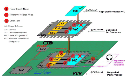
Figure 1. Integration of single ViC at SoC and PCB levels.
Basically, every ViC has its intrinsic robustness against interferences. In order to evaluate whether a ViC will perform as expected in the presence of interferences, Dolphin Integration is the only Silicon IP vendor to provide each ViC with its relevant tolerance templates. For example, as shown in Figure 2, the Power Supply Noise Tolerance Template (PSNT2) specifies the ViC immunity to power supply noise. The PSNT2 has a significant advantage over the Power Supply Rejection Ratio (PSSR) because it fully defines the ability of a ViC to tolerate power supply noise over a wide range of noise frequencies (up to several mega-hertz), whereas, in contrast, the PSRR just reflects how well a ViC can reject the power supply noise at one given noise frequency. The PSNT2 can then be compared to the Power Supply Noise Profile (PSNP), extracted from measurements, to evaluate whether the ViC performance is guaranteed or not. The comparison can easily be performed using our unique mixed-signal simulator SMASH [1].
As shown in Figure 2, the less noisy PSNP is within the immune region of the ViC PSNT2, thus the ViC performance is guaranteed, whereas the performance is not guaranteed for the noisy PSNP since it exceeds the ViC tolerance limit.
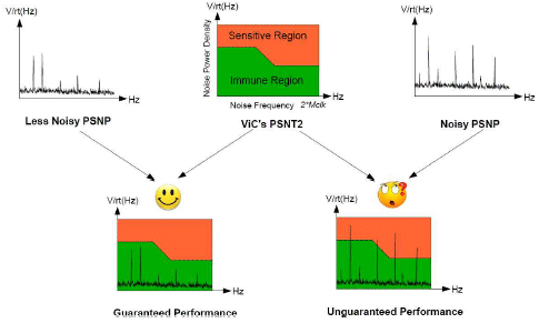
Figure 2. PSNT2 vs. PSNP in the frequency domain.
If unfortunately the interferences are too intense to be tolerated by the ViC, this may cause degradation of ViC performance and probably even the whole system. In order to relax these constraints to guarantee system performance during the integration process, Dolphin Integration has launched a novel integration strategy, namely SuperViC.
2. SuperViC for future
A SuperViC is a set of ViCs (two or more) which are provided readily assembled. It is a consistent combination of core ViCs connected with peripherals for dealing with critical issues such as noise propagated through the PRC&DN. As these ViCs and their interconnections are pre-defined and pre-optimized within the frame of the SuperViC assembly, they can be treated as a whole. Therefore, instead of having to put significant efforts into handling annoying interactions between each individual ViC, system integrators only need to deal with critical connections of the SuperViC with the PRC&DN and to the external world. With SuperViC approach, system integration risks and time-to-market are reduced while enhancing the partnership between ViC supplier and system integrator.
An important advantage of the SuperViC approach is that it provides a secure integration solution. In comparison with single ViCs, a SuperViC has relaxed tolerance templates by construction for power supply noise, clock jitter, reference noise… For example, a noisy power supply can result in performance degradation of a single ViC, whereas the same power supply may cause no harm to the SuperViC as it can tolerate more noise from the power supply without degrading its performance. In other words, a SuperViC is assembled to be more robust against interferences.
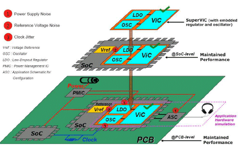
Figure 3. Integration of SuperViC at SoC and PCB levels.
As shown in Figure 3, it is important to point out that critical verifications of SuperViC are performed with recommended application schematics using the Application Hardware Simulation approach [2] on the targeted subsystem in order to further optimize system performance and reduce the BoM. The relaxed integration constraints of a SuperViC extend the possible choices of application schematics. Then, the most appropriate choice is not necessarily the most expensive one. This means that it is possible for customers to use less expensive application schematics which still achieve the performance requirements.
The advantages of the SuperViC approach that system integrators can benefit from are summarized below:
- Maintained performance of subsystem embedding ViC at system level
- Relaxed constraints for easy and secure integration
- Minimized BoM
- Reduced integration time and time to market
III. Simulation for relaxed PSNT2 of SuperViC
As previously stated, a SuperViC has relaxed tolerance templates (PSNT2, JT2...) in comparison with single ViC. In this section, we present a simple example with simulation results to illustrate the improvement of SuperViC tolerance to power supply noise.
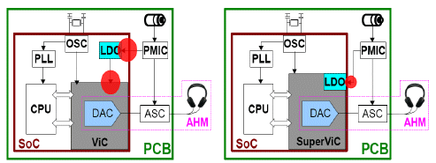
Figure 4: Impact of power supply noise (red-spots) on single ViC(left) and SuperViC (right)
Figure 4 illustrates the interference caused by the power supply noise (red-spots). On the left, the Low-Dropout Regulator (LDO) is integrated as a separate component with respect to the audio ViC. In this case, in order to appropriately power the ViC, the LDO must be optimized to not only sustain the noise coming from power source, but also to match the noise constraints of the standalone ViC.
Figure 5 shows the silicon results presented by SMASH of the Signal-to-Noise Ratio (SNR) degradation due to power supply noise. The audio ViC is expected to have an SNR performance of 95dB. The blue line represents its noise tolerance template (PSNT2). For less noisy power supply, the PSNP (green curve) lies below the ViC noise tolerance limit, thus the resulting SNR achieves the expected value. In contrast, if the power supply is noisier and parts of its PSNP (red curve) exceed the ViC tolerance template, the resulting SNR performance is degraded to 92dB.
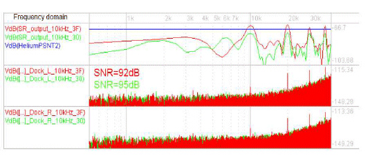
Figure 5. Proven risk of SNR degradation with PSNT2 due to power supply noise.
On the other hand, the right side of Figure 4 illustrates a novel arrangement in which the LDO is embedded within the audio ViC, thereby assembled as a SuperViC structure. In other words, the ViC is powered by its own embedded LDO. As the interaction between them has been optimized at SuperViC level, they behave as a whole with respect to other components in the SoC and PCB. As a result, the SuperViC only experiences noise coming from the power source. In addition, the risk of performance degradation caused by power supply noise can be significantly reduced because the SuperViC can tolerate more noise. This is illustrated in Figure 6, in which we can clearly see that the PSNT2 of the SuperViC (green line) is relaxed in comparison with the PSNT2 of the single ViC (blue line). In this case, the expected SNR value can be guaranteed even with a noisier power source as in the previous case.
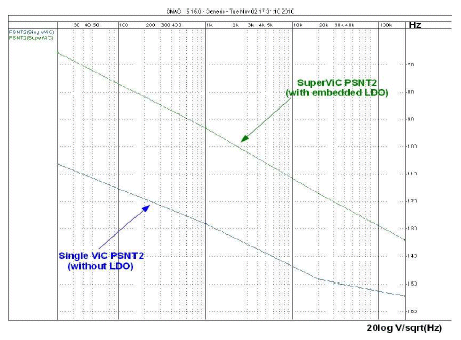
Figure 6. Relaxed noise tolerance limit of the SuperViC in comparison with single ViC.
IV. Heuristics for building PRC&DN Networks
The integration of ViCs or SuperViCs into a SoC requires properly addressing global integration issues through power, reference, clock and detector networks (PRC&DN). Building an efficient PRC&DN is mandatory to guarantee a high-performance system. The whole process consists in separately building the power network, reference network, clock network, and detector network then structuring all these networks together. The power network is going to be presented as an example to briefly explain our heuristics for building the complete PRC&DN.
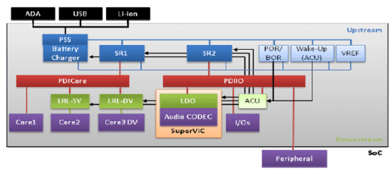
Figure 7: Typical SoC architecture with focus on power and reference networks
As shown in Figure 7, the power supply network is split into upstream (blue) regulators and downstream (green) regulators, connected through Power Distribution Interfaces (PDIs) (red). This approach allows splitting supply constraints between the loads (purple) and the sources, thereby allowing fast assembly of reliable P&RN using a set of predefined blocks. This enables to optimize the upstream regulators to deal with the source and the downstream regulators to deal with the loads.
Regarding the power network construction, some key points must be considered:
-
The network building starts from the loads to determine the number of required PDIs. The supply voltage, the Load Current Profile (LCP), the noise constraints (PSNT2), and modes of operation of each load must be taken into account. The loads must be grouped by types (digital or analog) and voltage level (core, IO, islet).
-
The optimization of the overall PRC&DN area is performed by gathering several loads onto one regulator.
-
Each hard block is delivered with its Electrical Performance Logic and Analog Model (EPLAM), Load Current Profile (LCP) and Power Supply Noise Tolerance Template (PSNT2).
-
Each downstream regulator is optimized using its parameterizable functional model, based on relevant parameters of its topology, to provide the appropriate Power Supply Noise Profile (PSNP) and Load Current Tolerance Template (LCT2), on the load side, as well as its LCP on the PDI side, with minimal power and area.
-
The upstream regulators and PDI physical implementation must be minimized to satisfy the noise constraints on the downstream branches and on the sources. Different options are available (linear regulators, inductor-based and inductor-less switching converters) based on efficiency needs, power dissipation constraints and other design priorities of the SoC.
-
The entire power network must then be analyzed for global efficiency, power dissipation, Bill of Material (number of external components), and pin-count, to determine if the power network is suitable for that application or if functional architecture changes are required.
Regarding the reference, clock and detector networks, the methodology and process for building them are in principle similar, all with the purpose of optimizing system performance by satisfying needs (e.g. LCP, supply voltage…), relaxing constraints (e.g. PSNT2, JT2, RNT2…) and reducing area and power consumption (share of regulators, reference…). It is important to underline that interactions among each network have to be seriously taken into account. For example, power supply noise not only affects the power network, but also impacts on the clock network (jitter profile). When all networks are successfully constructed, the structuring of the PRC&DN is performed from a global point of view on the whole system. Essential points must be considered and evaluated, such as the consequence of the Current Backward Transfer Function (CBTF) on each downstream branch – in particular for one sensitive to noise, dynamic and static IR drop, etc.
V. Conclusion
Based on the success of the Application Hardware Modeling (AHM) methodology introduced last year [2], a unique offering is launched this year – SuperViC. The AHM approach provides a methodology based on hardware modeling to assess through simulation the performance of a system function, i.e. a subsystem focusing on all the components that contribute to the function, across the boundaries of SoC and PCB, including sensors and actuators such as microphones and headphones or speakers. The goal of the SuperViC approach is to provide placement optimized and area optimized assemblies of ViCs that ease and secure the integration process by relaxing the integration constraints with maintained performances.
The application of the AHM approach during SoC integration secures the overall process from specification to application board. However, this approach is based on significant known-how related to the integration hot-spots, what effects need to be modeled, what modeling accuracy is required, how to restrict the simulation to the relevant subsystem… Therefore, in order to help customers deal with integration issues, the SuperViC approach is accompanied by specific Custom Training Packages (CTP) [3]. These packages include training and know-how transfer on modeling techniques, multi-level simulation principles… applied to the relevant hot-spots. Application engineers of such ViCs and SuperViCs can directly benefit from know-how transfer to securely deal with the integration issues plaguing this industry. Above all, such training packages aim at putting Application Engineers of ViC and SuperViC users in the best position for satisfying their own customers. This combination of SuperViC with CTP for AHM constitutes a unique offering, from which our customers and partners can benefit at once for right on first pass systems: high performance, safe integration and know-how development.
Reference
[1] Dolphin Integration, “SMASH User Manual”
[2] Dolphin Integration, “Application Hardware Simulation optimizing system functions for Multimedia Applications”, ICCAD 2009, Xiamen, China
[3] http://www.dolphin.fr/medal/smash/flash/smash_custom_TP.php
http://www.dolphin.fr/medal/smash/flash/smash_CTP.php
Related Semiconductor IP
- NPU IP Core for Mobile
- NPU IP Core for Edge
- Specialized Video Processing NPU IP
- HYPERBUS™ Memory Controller
- AV1 Video Encoder IP
Related White Papers
- Reconfiguring Design -> Adaptive computing makes efficient use of silicon
- Retargeting IP -> Silicon prototyping verifies IP functions
- Retargeting IP -> Design system compiles silicon straight from C code
- IP vendors making leap from source code to silicon
Latest White Papers
- Ramping Up Open-Source RISC-V Cores: Assessing the Energy Efficiency of Superscalar, Out-of-Order Execution
- Transition Fixes in 3nm Multi-Voltage SoC Design
- CXL Topology-Aware and Expander-Driven Prefetching: Unlocking SSD Performance
- Breaking the Memory Bandwidth Boundary. GDDR7 IP Design Challenges & Solutions
- Automating NoC Design to Tackle Rising SoC Complexity