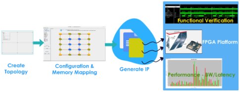
SignatureIP's iNoCulator Tool - a Simple-to-use tool for Complex SoCs
A Network-on-chip (NoC) is a network inside a System-on-chip (SoC) that connects to all IO, Compute and Storage devices. In addition to its networking function, the NoC also needs to do well in terms of power, performance and area. This is the logical part of the NoC and the not-so-difficult part of the game to meet the PPA needs. The most grueling part of the NoC design is physical implementation – to route it and meet the stringent timing requirements for the SoC design. This is the problem statement that motivated us to develop and introduce a tool that is designed from the ground up to solve the ever-growing complexities of the SoC’s network-on-chip– we call it the iNoCulator™ with the tagline NoC in a SNAP™.

The iNoCulator is a companion tool for silicon design engineers. This is an upfront enabler of how your silicon will look like upon implementation. The audience of the tool are silicon architects, logic design and physical design engineers who work on implementing complex interconnect matrices.
The silicon architects can explore topologies for power, performance and area (PPA) to pick and choose the optimal network for their needs. Physical design information is entered to experience how the PPAs play out, and how the iNoCulator provides a world of options for the architect to explore and evaluate.
The logic designers are able to generate the NoC RTL along with all simulation, integration and physical implementation collaterals. The implementation collaterals assist in chip level integration, synthesis and timing.
The physical designers influence the physical aspects of the NoC upfront during the design phase to ease routing and timing. This top-down approach addresses the physical implementation areas – routing congestion and timing closure. In the event of a physical design issue encountered in a late stage of the design, the changes to the NoC are incremental by doing a Knock the NoC ECO™. Usually, in the late stage of implementation, timing is closed at the subsystems but the issue comes at the chip top level. This is where the customer can update the chip top connectivity and adjust pipelining of the NoC, and thus contain the problem and the solution at the chip top level without opening up the subsystems. However, it is possible that there may be a late change required at a subsystem level. In such a scenario, the physical implementation engineer can regenerate the design only for the subsystem that requires change. Thus, the tool allows the SOC designers to go back and forth – incrementally and quickly between topology, design and implementation.
At SignatureIP, we listen to our customers, experience ground-level reality, and thus focus on bringing out state-of-the-art solutions. The R&D is focused on designing the NoC tool to be user-friendly – designed for system architects, logic designers and physical implementation engineers, and designed to close the gap between architecture, logic design and physical design. The tool is architected to scale and is designed for a dispersed team of engineers to work together collaboratively to come up with the optimal network for their silicon. Currently, the iNoCulator supports the non-coherent version of the SignatureIP NoC only. Our Coherent NoC will be added to the tool as we move forward. For more information, please visit https://signatureip.ai
Related Semiconductor IP
- Ultra-Low-Power LPDDR3/LPDDR2/DDR3L Combo Subsystem
- 1G BASE-T Ethernet Verification IP
- Network-on-Chip (NoC)
- Microsecond Channel (MSC/MSC-Plus) Controller
- 12-bit, 400 MSPS SAR ADC - TSMC 12nm FFC
Related Articles
Latest Articles
- Extending and Accelerating Inner Product Masking with Fault Detection via Instruction Set Extension
- ioPUF+: A PUF Based on I/O Pull-Up/Down Resistors for Secret Key Generation in IoT Nodes
- In-Situ Encryption of Single-Transistor Nonvolatile Memories without Density Loss
- David vs. Goliath: Can Small Models Win Big with Agentic AI in Hardware Design?
- RoMe: Row Granularity Access Memory System for Large Language Models