eTBc: A Semi-Automatic Testbench Generation Tool
Federal University of Campina Grande
Aprígio Veloso Avenue, 882, Bodocongó
Campina Grande - PB - Brazil
ABSTRACT
This paper presents a semi-automatic testbench generation tool called eTBc and a methodology called VeriSC (which allows for testbench simulation before RTL without additional code writing). This resources can be used in IC-development flow in order to enhance productivity on verification tasks through automatic generation of testbench prototypes. The case study is the DigiSeal circuit for the detection of tampering with energy meters.
1. INTRODUCTION
The implementation of testbenches can take a considerable amount of time in the verification process. Some reasons, which can increase the time for testbench implementation, are the number of connections between modules/ blocks, the time spent to adapt the testbench to the Design Under Verification (DUV) and the number of module instances, transaction data structures and transaction communication channels.
A methodology that makes the complex verification process easier and a tool to implement this methodology and generate automatically testbench prototypes can be a good approach to reduce the overall time of project flow. This paper presents a semi-automatic testbench generation tool eTBc ( Easy TestBench Creator ), which has been used to generate testbench prototypes for the DigiSeal project [1].
The remainder of this paper is organized as follows. Section 2 presents the VeriSC [2] methodology, Section 3 describes the eTBc tool, Section 4 shows the DigiSeal case study, Section 5 shows some results and Section 6 concludes the work.
2. THE VERISC METHODOLOGY
VeriSC is a functional verification methodology, which defines a better integration between the RTL implementation and verification. Through this methodology, testbenches are implemented before or along with the RTL implementation, as shown in Figure 1. The Figures 1 and 2 shows a comparison between VeriSC project flow and a traditional (common) project flow. In the Figure 1 the testbench implementation can be done before or in parallel with the DUV implementation. With this approach it is possible to use the testbench to make the debugging, without any extra code. On the other side, in the second flow it is necessary to first implement the DUV and then the testbench.
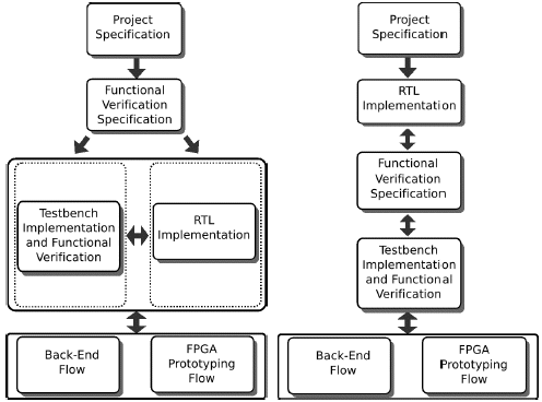
Figure 1: VeriSC Methotology Flow Figure 2: Traditional Methotology Flow
There are many advantages on using this approach shown in Figure 1. First of all, the functional verification is performed incrementally throughout each iteration of hierarchical refinement. The verification process is usually more efficient when the hierarchical subdivision is done from a verification perspective. As most of the projects effort is concentrated in the verification process, the overall design effort decreases significantly. Other advantages are reuse employed in a way to assure interface consistency throughout the hierarchical decomposition process; and finally, testbench and DUV design errors are detected and debugged earlier, reducing overall debugging time. In traditional design methodologies, the DUV is implemented before the testbench. In this way, a considerable effort is needed to adapt the testbench to the DUV, because the DUV is already implemented.
The RTL design engineer shall have a complete environment to test his/her RTL code right from the beginning and the verification can proceed prior or in parallel with the implementation of the design. Traditional methodologies allow testbench implementation before DUV implementation only by using an extra code that has to be written to represent the DUV. This code is not reused later in functional verification where the DUV is present. To the best of our knowledge, there is no other methodology capable of providing a testbench beforehand using only a code that is needed also for the final testbench with the implemented DUV. The general testbench scheme used in VeriSC is shown in Figure 3.
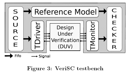
The testbench is composed of the following elements: Source, TDriver(s), TMonitor(s), ReferenceModel (RM) and Checker. The functionality of each block of the testbench is briefly described below. More details can be found in [3], [2] and [4].
-
The synchronization mechanism of the testbench is implemented by means of First-In-First-Out queues (FIFOs), through transactions. The testbench structure shown is intended to be used only for synchronous designs with a single clock signal.
-
Source: it is responsible for providing transaction level (TL) data to the DUV and to the RM. It is connected to the RM and to the TDriver(s) by means of FIFO(s). There is one FIFO for each input interface of the DUV. The same number of FIFOs is going to the RM and to the TDrivers.
-
TDriver: it receives TL data from the Source, translate it into specified protocol signals and passes these signals along with the required data to the DUV. A TDriver functions as a bridge between TL and signal level. There is always one TDriver for each input interface to the DUV.
-
TMonitor: it is a bridge between the signal data and transactions. Thus, it is responsible for receiving the protocol and data signals from the DUV and transforming them into TL data. The TMonitor puts the TL data into a FIFO and passes them to the Checker. There is always one TMonitor for each output interface to the DUV.
-
Checker: it is responsible for comparing TL data coming from the RM with TL data coming from TMonitor( s) to see if they are equivalent. The checker will automatically compare the outputs from RM and DUV and prints error messages if they are not equivalent.
-
Reference Model (RM): it receives TL data from the Source through FIFO(s) and sends TL data to the Checker through FIFO(s). If not provided by a third part, the verification engineer must implement the functionality of the RM.
Following, the eTBc testbench generation tool will be described.
3. eTBc TOOL
The Easy Testbench Creator (eTBc) is a tool for semiautomatic testbench generation. This tool works as a code generator, receiving two files as input:
-
A Transaction Level Netlist (TLN) file described by the functional verification engineer (user of eTBc). This file is a model of the IP-core using Transaction data and RTL data. The RTL data used in this level is only the name of modules I/O ports. The remaining of the description is only transaction data. The language used in this level is eTBc Design Language (eDL). eDL is a simple language used to describe modules, connections, FIFOs and some data in the RTL level.
-
A template of a testbench element that will be generated. The eTBc template is a way that eTBc works to generate testbench elements. The role of templates is to guide eTBc to generate code, based in one TLN. The TLN defines the model of system and template defines the model of testbench. The templates are created using eTBc Template Language (eTL) and there are implemented templates in VeriSC methodology for SystemC and Verilog languages. eTL is a language that allows adjustment to a specific methodology and HDL. If a Verilog/SystemVerilog, VHDL or SystemC specific methodology wants to generate testbenches in a specific way, a template can be written using eTL for this purpose. The disadvantage of this approach is that eTL must be learned.
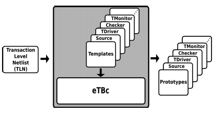
Figure 4: eTBc Architectural Model
As can be seen in the architectural model of the tool presented in Figure 4, the models are created using the eTBc Design Language (eDL). Internally the tool uses a code generator and two translators, one to interpret the TLN code and the other to interpret the code of the templates. The eDL language is used to write the TLN code to describe the model. The eTL language is used to write the templates used by the tool. If one wants to port the tool for an specific methodology, he has to create new templates according with this methodology.
The eTBc can be adapted to other methodologies and languages using the template language (eTL). In this case, the verification manager/team has to implement your own templates to use with a specific methodology. An simple example of TLN written in eDL is shown in Source Code 1. This TLN is a model of an 8-bit adder. The declaration of line 1 is a ”struct” called data which defines the transaction level and RTL informations. In this case, there is a declaration at line 5 that is used to generate transaction level information in testbench. In this case, according with VeriSC methodology, any ANSI C++ [5] data type can be used.
At the line 10, there is RTL information that defines 8-bit width signal. This RTL information is used to generate a wrapper of Design Under Verification (DUV) in Verilog according with VeriSC methodology. This wrapper is an initial prototype of the adder module with only I/O ports and it need to be completed by a RTL engineer. At the line 15, the toplevel module adder is declared with two inputs (a,b) of ”data” type and one output (s) of same type. These declarations are I/O transaction ports. The declarations at lines 16,17 and 18 means only I/O transaction ports, not RTL ports. After creating the model, the engineer (user) of eTBc can generate all testbench elements (prototypes) running eTBc one time for each prototype to be generated. After that, in order to finish the testbench, the user need to fill the ”source”module of VeriSC with stimuli generation and ”checker” with all asserts constraints according with the verification plain.
Source Code 1: File example.tln
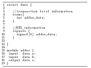
From this example shown in Source Code 1, eTBc can generate all testbench elements of the VeriSC methodology discussed in section 2. This model written in eDL is not restricted only to VeriSC methodology. It can be used in any verification methodology. To use this model with an other methodology is necessary others templates written in eTBc Template Language (eTL).
An example of template can be seen in Source Code 2.
Source Code 2: File template example.txt
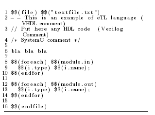
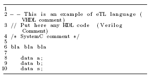
The Source Code 2 uses eTBc Template Language (eTL). In this example, the line 1 defines a file name ”textfile.txt”. This tells to eTBc to generate a file named textfile.txt. The Lines 2,3,4 and 6 are any text that will be bypassed to output file shown in Source Code 3. Keywords in eTL are declared as $$(etl keyword). So the lines 1, 8-10,12-14 and 16 in Source Code 2 are keywords in eTL. Templates written in eTL uses TLN information to produce output files. So, the lines 8-10 tells to eTBc to iterate in all input declarations of the module adder shown in Source Code 1. The lines 8,9 and 10 of the output file textfile.txt are the result of lines 8-10, 12-14 of Source Code 2. In eTL, ”foreach” loops are indexed with variables i and j as shown in lines 9 and 13 of Source Code 2.
This is a simple example how to eTBc handle templates in order to generate code.
Source Code 3: File textfile.txt
In Brazil, violations on the electric power network committed by customers cause an estimated loss of 20% of the country’s energy production, and as a consequence, a reduction of revenues of the electric power distribution companies. Therefore, there is a great need for solutions that would minimize this problem.
The DigiSeal project had the objective of implementing a circuit for the detection of tampering with energy meters for electric power distribution installed at customer homes. This device should minimize electric power thefts and reduce maintenance and repair costs. It should also reduce the number of energy failures due to an overload in the transmission network [1].
This circuit has a sensor to detect the opening of the meter box and a RF transceiver [6] to inform a palmtop computer (PDA - Personal Digital Assistant). The whole system works as follows: the DigiSeal installed in the box will be monitoring the violation detector and store a certain number of violation events with time and date. The RF data transmission will only take place if it receives a status request from a PDA within the area. The PDA used by the controller sends a status request to the DigiSeal. The DigiSeal sends its identification and status information (”OK”, ”VIOLATED”or ”INMAINTENANCE”) back to the PDA. Then, the DigiSeal can send the list of violation events to the PDA on request.
In order to achieve the overall system project´s objective, the DigiSeal needs to be able to capture the position of an electric switch connected to the lid of the power meter box which acts as violation detector, perform cryptography and forward error correction (FEC) [7, 8] for RF communication and interfacing to a RF transceiver.
In Figure 5 can be seen the transaction level schematic of the DigiSeal that works in the following way: data comes encrypted with transmission errors through the transaction RFrequest to the FEC block that uses the Golay [9] algorithm to correct it. Then, through the CRIPTrequest transaction, the data enters the Cryptor that decrypts it using the DES protocol [10]. At this time, the data will go through the Request transaction to enter the StateMachine block where the DigiSeal status and a history of violation events are stored. The sensor switch is connected to this block. Next, the data exits through the Reply transaction. It enters the Cryptor block to be encrypted. Finally, the data goes out through the CRIPTreply transaction to the EEC block, which implements the Golay error code generation algorithm. Then the data leaves through an RFreply transaction. The blocks of the DigiSeal (Figure 5) were coded in Verilog. The SystemC was used for the reference models and testbenches.
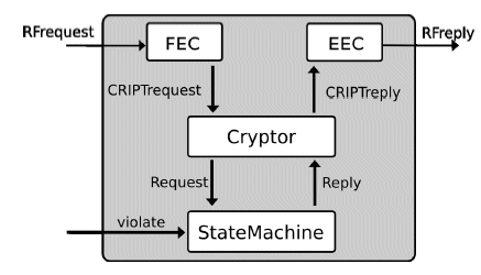
Figure 5: DigiSeal Transaction Level Model
A portion of TLN of digiseal is shown in Source Code 4. This TLN is an source written in eTBc Design Language (eDL). The Figure 5 shows the graphical model of this TLN.
Source Code 4: File digiseal.tln
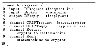
The I/O declarations is at lines 2-4 that defines de transaction input/output of the digiseal module. The declarations at lines 6-9 are channels used to comunicate internal modules using transaction data. The type of each I/O and channel was defined in individual ”struct” not shown in Source Code 4.
5. RESULTS
VeriSC methodology was used in many projects. It was used to implement the chips which won the IP/SOC 2006 Best Design Paper Award [3]. In this specific case study, eTBc was used together with VeriSC. Then, very good results appear. In order to assure the benefits of using eTBc together with VeriSC, the same engineer that made all the process of functional verification manually, used later eTBc in order to implement the same work environment.
The eTBc tool was applied in all functional verification steps of the VeriSC methodology. After that, was created the TLN of the DigiSeal using the eDL language and random stimuli generators were placed in testbench of the DigiSeal. Then was analyzed the times for automatic testbench prototypes conception using the eTBc tool and without using it. Testbench prototypes are elements wich compose all the VeriSC methodology steps. They are sames for all projects that uses this methodology.
Using eTBc, the time spent to create the DigiSeal TLN and to generate testbench prototypes was two hours. After that, fifteen hours were necessary to fill the testbench with the random stimuli generators. So, the total flow using the eTBc tool was seventeen hours.
Without using eTBc tool, the same engineer has spent one hundred and two hours to create the same testbench prototypes conception flow.
The conclusion is that, with the use of eTBc tool the production profit was 83,33% faster than the manual process. So, the eTBc tool can speed up the process of functional verification. The table 1 presents comparison of some vantages and disadvantages of using the eTBc tool.
| With eTBc | Without eTBc |
| Semi-autimatic testbench implementation | Manual testbench iplementation |
| Flexible adapt to other methodologies and verification languages | Difficult adapt to other methodologies and languages |
| Speed up in verification proccess | Same Verification time |
| Learn eDL | language Additional knowledge is not necessary |
Table 1: eTBc and VeriSC advantages
The DigiSeal FPGA implementation was fully functional at the first attempt, proving the efficiency of the methodology and tool adopted. For area estimation, a silicon layout for Austriamicrosystem’s C35B3 technology [11] was generated using Astro from Synopsys [12] (see Figure 6). The resulting area was 2.2 × 2.2mm2, as reported in Table 2.
| Characteristics | DigiSeal |
| Testbench code line number | 45341 |
| RTL code line number | 3112 |
| Logic gate count | 6176 |
| Silicon area | 2, 41 × 2, 41mm2 |
Table 2: DigiSeal Characteristics
6. CONCLUSIONS
The tool eTBc is based on VeriSC methodology which was used to validate high complex IP-cores [3]. eTBc is on continuous development and the roadmap plain is to implement
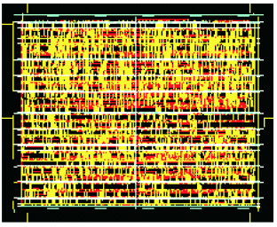
Figure 6: Layout from DigiSeal project
a graphical user interface, specific templates for more verification methodologies. Based on the DigiSeal case study, the testbench generation saved time was 83% compared to the manual process. The important contribution given for eTBc tool was the speed up in the functional verification, which is one of must critical areas in the IP-core development process.
7. ADDITIONAL AUTHORS
Additional authors: Matheus B. E. Rodrigues , Maria de L. N. Neta, Fabr´ýcio G. L. Melo, Helder F. A. Oliveira, email: (matheus,maria,fabricio,helder)@lad.dsc.ufcg.edu.br
8. REFERENCES
[1] Ana Karina Rocha and Elmar Melcher. Digiseal - an application using functional verification with timed transactions. 2006.
[2] K. R. G. da Silva, E. U. K. Melcher, I. Maia, and H. do N. Cunha. A methodology aimed at better integration of functional verification and rtl design. Design Automation for Embedded Systems, accepted for publication in a Special SystemC Edition, 2006.
[3] Ana Karina Rocha, Patricia Lira, Yang Yun Ju, Edna Barros, Elmar Melcher, and Guido Araujo. Silicon validated ip cores designed by the brazil-ip network. IP/SOC, 2006.
[4] K. R. G. da Silva, E. U. K. Melcher, and G. Ara´ujo. An automatic testbench generation tool for a systemc verification methodology. SBCCI - 17th Symposium on Integrated Circuits and System Design, 2004.
[5] ISO/IEC 14882. Programming Languages - C++, 1998.
[6] Texas Instruments. Single Chip RF Transceiver TRF 5901
[7] W. Stallings. Cryptography and Network Security - Principles and Practices, 3rd ed., Prentice Hall. 2003.
[8] D. Stinson. Cryptography Theory and Practice, 2nd ed., CRC Press. 2002.
[9] R. H. Morelos-Zaragoza. The Art of Error Correcting Coding, John Wiley & Sons. 2002.
[10] R. Usselmann. DES/Triple DES IP Cores.
[11] Austriamicrosystems A. G. A c35 cmos process parameters, doc. eng-182, revision: 4.0, 12/2005.
[12] Astro. Astro advanced placement and routing solution for system-on-chip designs, synopsys, inc., 2005.
Related Semiconductor IP
- NPU IP Core for Mobile
- NPU IP Core for Edge
- Specialized Video Processing NPU IP
- HYPERBUS™ Memory Controller
- AV1 Video Encoder IP
Related White Papers
- Automatic C-to-VHDL testbench generation shortens FPGA development time
- Resolution of Interoperability challenges in Automatic Test Point insertion across different EDA vendors
- Paving the way for the next generation audio codec for the True Wireless Stereo (TWS) applications - PART 1 : TWS challenges explained
- Paving the way for the next generation audio codec for True Wireless Stereo (TWS) applications - PART 2 : Increasing play time
Latest White Papers
- Ramping Up Open-Source RISC-V Cores: Assessing the Energy Efficiency of Superscalar, Out-of-Order Execution
- Transition Fixes in 3nm Multi-Voltage SoC Design
- CXL Topology-Aware and Expander-Driven Prefetching: Unlocking SSD Performance
- Breaking the Memory Bandwidth Boundary. GDDR7 IP Design Challenges & Solutions
- Automating NoC Design to Tackle Rising SoC Complexity