Electronic Circuit Design for RF Energy Harvesting using 28nm FD-SOI Technology
By M. Awad, P. Benech, J-M. Duchamp (Institut de Microélectronique Electromagnétisme et Photonique et le Laboratoire d'Hyperfréquences et de Caractérisation (IMEP-LaHC), Polygone scientifique MINATEC)
Abstract
A design of voltage doubler circuit has been studied in context of electromagnetic energy harvesting using 28 nm FD-SOI technology. After analysis of the operating constraints of the circuit, the choice was made in favour of NLVT transistor configured as a diode. The design and optimization of the circuit is presented as well as the influence of the polarization of the substrate.
1. Introduction
The transfer of electromagnetic power wirelessly over a distance was not possible in 19th century, since the electronic systems like autonomous sensors with ambient RF energy were not available. Recently, in 21st century such electronic circuits have been developed. Moreover, the exponential increase in number of Wi-Fi access points over the last 5 years induces levels of RF power density of up to 10 nW / cm2 [1], and a power captured by a Wi-Fi patch antenna is about 150 nW. At the same time, the performance improvement of the microelectronics made it possible to reduce the standby currents of the microcontrollers to 20 nA for a voltage of 1.8 V, i.e., 36 nW (PIC16LF72 nW from Microchip). Therefore, it is possible to support the power consumption by RF energy harvesting. For this it is necessary to use a non-linear element (a diode) to convert the RF signal to a DC electrical signal up to -40 dBm @ 2.45 GHz [2]. These diodes are often associated in voltage multipliers to achieve a sufficient voltage of 1V. A sensitivity of -27 dBm has even been demonstrated in CMOS technology 0.18 µm [3].
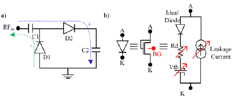
The aim of this paper is to study and design a voltage doubler circuit (Figure 1) for the RF energy harvesting using 28 nm FD-SOI technology. Furthermore, to explore the impact of polarization of substrate on parameters of the nonlinearity (threshold, losses and leaks).
2. RF voltage doubler and FD-SOI technology
2.a. Structure et principe
Dickson voltage multiplier for radio frequency (RF) energy harvesting, shown in Fig.1-a, is simple and has an improved performance compared to other existing topologies (for energy harvesting). The non-linear components in Dickson multiplier are realized using MOS transistor in 28nm FD-SOI technology.
The arrangement shown in Fig.1-a makes it possible to rectify the two half-waves of the input RF signal. When the voltage is negative, the capacitor C1 is charged through diode D1. Further, when the input voltage becomes positive, capacitance C2 stores the charges resulting from the sum of the input voltage and the voltage across C1 via D2.

Fig. 1. Voltage doubler (a) and transistor like diode model (b)
In case of ideal diodes, the final voltage transferred to C2 without output load is equal to 2VRF,max. Furthermore, it is easy to determine that the output voltage of such n-stage multiplier (without load) with diodes, for which only the threshold voltage imperfections are considered. In that case, the output voltage is given as:
Vcn=n(VRF,max−Vth)
Generally, Schottky diode are used for RF energy harvesting application owing to the low threshold voltage and high efficiency. However, Schottky diodes cannot be integrated. Therefore, Schottky diodes are replaced by transistor like diodes, where the gate is connected to the drain. In CMOS transistor, the threshold is high and there exist a number of parasitic parameter. Hence, FD-SOI technology is used. The non-linearity can be controlled by polarizing the Back Gate (BG) (Fig1-b). This polarization affect the threshold voltage, dynamic resistance and leakage current which will be explained in the subsequent section.
2.b. Technology and transistors
Dimension reduction of the transistors with respect to the thickness of the silicon substrate (bulk) induces undesirable parasitic effects which degrade their performances. To circumvent these disadvantages, FD-SOI technology has been developed. Owing to Buried Oxide insulation placed between the substrate and the
active part of the transistors (Fully Depleted), this technology reduces the different types of leaks and losses in the substrate. Moreover, because of the "BOX", the substrate can be seen as another gate, known as a back gate (BG). The polarization of BG makes it possible to modify the parameters of the transistor. In the FD-SOI 28 nm technology, four types of transistors are available: NLVT, PLVT, NRVT and PRVT, where LVT stands for "Low Voltage Transistor" and RVT for "Regular Voltage Transistor".
3. Conception and simulation results
3.a. Choice of the transistor
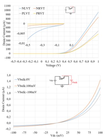
FIG. 2-a reveals the I-V characteristics of NLVT, PLVT, NRVT and PRVT configured like diode. Note that NLVT has the smallest threshold voltage and the lowest series resistance, however, it has the highest leakage current. Moreover, the increase in the polarization of the BG makes it possible to reduce the threshold voltage as shown in FIG. 2-b.The results suggest that the best choice is NLVT to configure the diodes, since they exhibt low threshold voltage.

Fig. 2. I-V curves of the transistors (a) and for different substrate voltage (b)
3.b. Simulation results of the voltage doubler
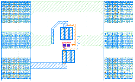
The performance optimization of the voltage doubler is linked to the appropriate choices of electrical parameters of the transistors mounted on diodes (Di) (e.g., threshold voltage, leaks, losses, parasitic capacitances, etc.). These parameters can be obtained from the geometrical dimensions of the transistors. The simulations of the circuit are performed using microelectronic design software (Cadence®). The capacitance value (Ci) is set to 10pF to achieve a compromise between the amount of charge stored and the charge time. The design of voltage doubler using 28nm FDSOI technology is presented in Fig. 3.

Fig. 3. Doubler layout using FD-SOI 28nm
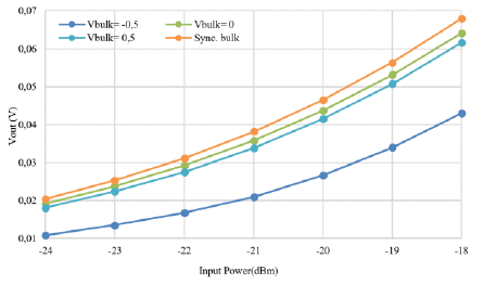
FIG. 4 shows the variation of the output voltage of the doubler as a function of the input power for different BG voltages. For the same RF input power, the output voltage obtained for a positive polarization of the BG is greater compared to when BG voltage is negative. However when the BG is connected to the ground, the output voltage of doubler is even larger the voltage obtained for positive polarization of BG.
However, there exists a better polarization solution, as shown in FIG. 4, which consists of varying the BG voltage as a function of the operating mode of the transistor D2. Indeed, if the input voltage is positive (VBG), the threshold is reduced for passing D2. Also, when the voltage changes sign, VBG becomes negative and leakage of blocked D2 is reduced.

Fig. 4. Output voltage as input power and BG voltage polarization
4. Conclusion
This article presents the design of a voltage doubler optimized using FD-SOI technology. Among the transistors, the most suitable is the NLVT because of its lowest threshold voltage. Moreover, the polarization of the BG influences the performance of the transistor and makes it possible to design low-threshold and low-leak diode connected transistor.
References
[1] Internet site «RF spectral survey in London: Measurements at the Mile End metro station», http://www.londonrfsurvey.org/
[2] C. H. P. Lorenz et al., «Breaking the Efficiency Barrier for Ambient Microwave Power Harvesting With Heterojunction Backward Tunnel Diodes», in IEEE MTT, vol. 63, no. 12, pp. 4544-4555, 2015.
[3] M. A. Abouzied et al., «Low-Input Power-Level CMOS RF Energy-Harvesting Front End», in IEEE MTT, vol. 63, no. 11, pp. 3794-3805, 2015.
Related Semiconductor IP
- NPU IP Core for Mobile
- NPU IP Core for Edge
- Specialized Video Processing NPU IP
- HYPERBUS™ Memory Controller
- AV1 Video Encoder IP
Related White Papers
- RF Simulation Improves 802.11a System Performance
- RF system-in-package competes with SoCs
- Tailoring is critical to successful RF analog CMOS chips
- Adaptive silicon comes to RF
Latest White Papers
- Transition Fixes in 3nm Multi-Voltage SoC Design
- CXL Topology-Aware and Expander-Driven Prefetching: Unlocking SSD Performance
- Breaking the Memory Bandwidth Boundary. GDDR7 IP Design Challenges & Solutions
- Automating NoC Design to Tackle Rising SoC Complexity
- Memory Prefetching Evaluation of Scientific Applications on a Modern HPC Arm-Based Processor