Rethinking The Pursuit of Moore's Law
By Nick Kepler, SuVolta
Introduction
There is much excitement about the semiconductor industry moving to 28nm and 20nm process technology. For a majority of products, however, it will be several years before these leading-edge process technologies make economic sense. These products will remain on mature process technologies, getting none of the benefits that Moore’s Law1 brings. What if there was another way? What if you could extend the capabilities of mature technologies without having to overcome the cost wall of a shrink to the leading edge?
The immediate pursuit of Moore’s Law makes sense for companies that require the performance and density that come with leading-edge process technology, and that can afford the costs of creating large, high-performance products such as CPUs, GPUs, FPGAs, and APUs. On the other hand, a majority of IC products are very cost-constrained, and do not require leading-edge performance and density. These products would benefit from a technology roadmap that reduces power consumption while delaying a transition to next-generation process technology until the migration cost is lower.
This article argues that the benefits of Moore’s Law can now be split in two: the classical benefits of greater density and lower cost-per-transistor from shrinking, and the benefit of extending the capability of mature process technology generations by reducing power consumption. SuVolta’s Deeply Depleted Channel™ (DDC) CMOS transistor, which offers a 50% reduction in power consumption, is an example of a technology that can enable such an extension. Specifically, considering that a migration to the next technology generation reduces power by 25-30%, the DDC transistor can extend the 65nm generation to the same power consumption reported for conventional 28nm process technology.
This technology extension is important, because lowering power consumption creates end-market value for an IC product. While there are extension costs, they are minimal compared to leading-edge migration costs. An effective technology extension delays the significant cost of technology migration by retaining the mature design rules, design methodologies and circuit IP, and manufacturing tool sets of the mature technology.
The cost of keeping up with Moore’s Law There is always a cost associated with switching process technologies. The costs of migrating to leading-edge process technologies is well documented in terms of the need for new manufacturing tool sets and design IP as well as design and mask technologies. But migration is also expensive because it runs into the steep portion of several learning curves: the cost-of-entry learning curve, the first-time-failure learning curve, and the die-cost learning curve. For a majority of products it makes economic sense to delay the cost of migrating to leading-edge process technology.

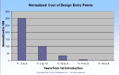
Figure 1: Cost-of-entry for 90nm through 40nm process technologies
The cost-of-entry learning curve, illustrated in Figure 1, shows that early adopters of a new process technology generation pay significantly more entry costs than adopters who wait. Cost-of-entry refers to the non-recurring engineering (NRE) costs associated with migrating to a different process technology generation, including design migration, third-party design IP, masks, and package development. The data is a blend of entry costs from 90nm through 40nm for many products compiled by VLSI Research. On average, the cost-of-entry decreases by 5x in the first four years after the introduction of a new process technology generation as the early adopters drive the maturity of the items mentioned. The cost savings obtained by delaying migration are extremely important for products that don’t have the huge volumes and/or high average selling prices (ASPs) needed to amortize the cost-of-entry at introduction of a new process technology.

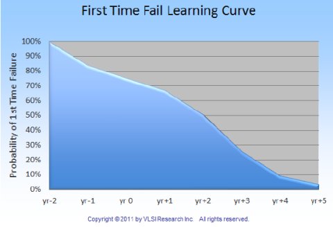
Figure 2: First-time-failure learning curve for 90nm through 40nm process technologies
First-time-failure rates are another important reason to delay migration. First-time-failure refers to the percentage of products that have to re-spin silicon for any reason, such as timing or Design for Manufacturing (DFM) failures. First-time-failure rates decrease by 8x in the first four years after the introduction of a new process technology generation, as shown in Figure 2 (the data behind Figure 2 is also a blend from 90nm through 40nm for many products, compiled by VLSI Research). Most of this decrease is the result of improved manufacturing maturity and better understanding of design/technology interactions.
Re-spins caused by first-time failures add direct design, mask, and fab processing costs. In addition, re-spins also delay product introductions, eliminating early revenue streams at a time when product prices are highest. Note that year 0 in Figure 2 is the point of first product introductions, and the delays from re-spins are so significant that the earliest design starts are as much as two years ahead of production introduction. Again, this highlights the value of delaying the migration into a new process technology generation for products that don’t need leading-edge density.
The amount of money at risk is increasing with each process technology generation because the complexity of each generation is increasing. For example, the complexity of deep-submicron process technologies eliminated simple, direct scaling of design rules several generations ago -- and therefore simple, direct scaling of product designs. In addition, more restrictive design rules are added to each new technology generation to overcome manufacturing effects of the smaller geometries. As a result, it is no longer simple and inexpensive to migrate IC products to each new technology generation. Instead, increasing amounts of redesign work are needed to achieve Moore’s Law scaling of a product design into the next technology generation to accommodate the altered design rules, and this migration of the design costs both money and time. This increase in the amount of money at risk when migrating design is a strong motivator to embrace technology extensions for products that don’t require a large increase in feature density and/or don’t have huge volumes.

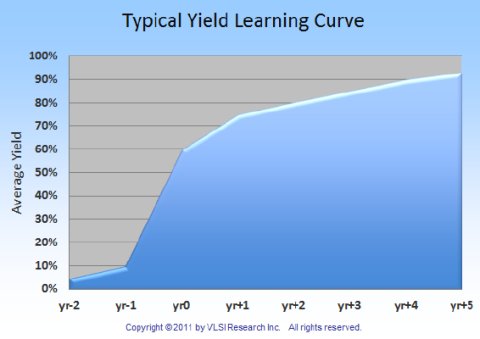
Figure 3: The manufacturing-yield-learning curve

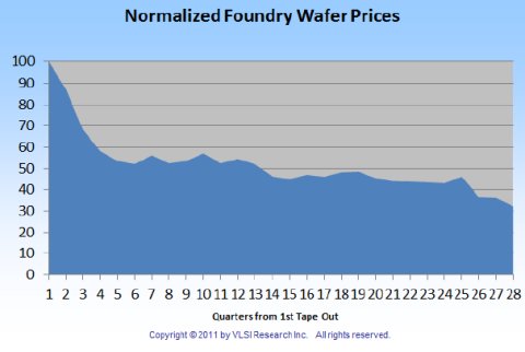
Figure 4: The wafer-price curve
Figure 3 illustrates the manufacturing-yield-learning curve and Figure 4 illustrates the wafer-price curve, again blending data from 90nm through 40nm for many products. The die-cost learning curve, which is what most products focus on, is a combination of these curves and supply-and-demand. The result is higher die prices for products that are produced in the first several quarters of production of a leading-edge process technology. This effect is expected to be particularly strong for the 28nm generation because limited supply is expected to keep 28nm wafer prices well above $6,000 throughout 2013.

Figure 5: A case study of product migration to leading-edge process technology
The specific case summarized in Figure 5 highlights the challenge of migrating a product to leading-edge process technology. This product is the second generation version of a processor-type product that is currently in production using mature 65nm process technology. The fabless company that makes this product is evaluating what process technology to use for the second generation (the company has asked to remain anonymous). The expectation is that several million units will be sold each year for a mobile application, generating approximately $100M in annual revenue. Under these circumstances, spending approximately one million dollars of NRE to create the design IP and masks necessary for this product in 65nm process technology is acceptable, but the several million dollars of additional NRE expense to migrate from 65nm to 40nm or 28nm design IP and masks is prohibitive. In addition, while the migration to 40nm or 28nm would provide a significant power reduction, the performance improvement is minimal. Finally, the higher wafer cost and lower yield maturity for 40nm and 28nm process technology, combined with the area of this 4x4mm 65nm product being pad-limited in 40nm and 28nm process technology, result in a process technology migration to 40nm or 28nm leading to an increased die cost. Products that are not pad-limited in scaling to 40nm and 28nm would see a reduction of approximately 40% and 60% in die cost, but this would not be sufficient to offset the increased NRE cost and provide an acceptable gross margin.
Not surprisingly, the migration cost to 20nm process technology will be even greater than to 28nm process technology. Patterning costs will increase dramatically for 20nm process technology because the delay of EUV lithography means that many layers will require double-patterning with 193nm immersion lithography tools. As a result, 28nm will most likely be a long-lived process generation.
The excessive costs of migrating to leading-edge process technology argue for keeping many products in mature process technology generations. However, to remain competitive mature process technologies need to extend their value in addition to providing a way to delay the cost of migrating to newer technology. Reducing power consumption is a particularly good way of extending the value of mature process technologies because a majority of today’s IC products are very power-constrained. The amount of functionality that can be packed into mobile computing devices such as smartphones, tablets, and notebooks is now limited by power consumption. In addition, power density will soon limit process technology applications from CPUs in server farms to small ICs stacked together in 3-D packages because of the amount of heat generated.
To remain competitive a mature process technology must reduce power consumption by at least 25-30%, which is the amount usually saved by migrating to next-generation process technology. One approach to reduce power consumption by this much is to lower the power supply voltage VDD. Another approach is to implement a transistor technology that addresses the primary cause of power consumption in deep submicron process technology: variation in transistor threshold voltage (VT). SuVolta’s DDC CMOS transistor technology takes both of these approaches to reduce the power consumption of CMOS ICs by 50% or more while maintaining performance. The DDC transistor’s channel structure reduces VT variation by up to 50% compared to conventional transistor technology, enabling scaling of supply voltage (VDD) by 30% while maintaining the same system clock speed and reducing overall leakage. These benefits apply across a wide range of integrated circuit (IC) products, including processors, SRAMs, and SOCs that are critical across the consumer and mobile markets.
An extension of a mature process technology is only valuable if it avoids the migration cost associated with migrating to the leading-edge process technology. SuVolta’s planar, bulk DDC transistor avoids this migration cost because it is compatible with current manufacturing and design infrastructure. It leverages existing CMOS design rules and process flows, and can be manufactured in existing fabs because it does not require new equipment or new materials. Furthermore, chip designs with SuVolta’s technology use conventional design tools and design flows. As shown in Figure 6, SuVolta’s technology would allow the product illustrated in Figure 5 to reduce power consumption by 50%, similar to 28nm process technology, while avoiding the 500% NRE cost of 28nm process technology relative to 65nm process technology.

Figure 6: A case study of product migration to leading-edge process technology and the DDC transistor
Conclusion A majority of products remain on mature process technologies because of the high costs of migrating to leading-edge process technologies. These products would benefit instead from extending a mature process technology generation to have lower power consumption while delaying the cost of migrating to leading-edge process technology until the steep portion of the cost-learning curve is past. This technology extension benefit will remain true as the specific process technologies that are classified as “mature” (90nm and 65nm today) and “leading-edge” (28nm today) change over time.
To learn more about SuVolta’s DDC transistor technology, please visit www.suvolta.com/Technology/Technology-Overview/.
About the Author
Nick Kepler is Vice President of Products for SuVolta. Prior to joining SuVolta, Kepler spent 22 years in a variety of management and technical roles at Advanced Micro Devices concluding with Vice President, Advanced CMOS Process Technology Development followed by three years in executive-level positions at GLOBALFOUNDRIES.
1 Moore’s Law states that the number of transistors on an integrated circuit (IC) will double every two years, driving the cost-per-transistor down. These efforts have also brought electrical performance and power benefits that, while not strictly Moore’s Law, are significant in the additional value they bring.
Related Semiconductor IP
- UFS 5.0 Host Controller IP
- PDM Receiver/PDM-to-PCM Converter
- Voltage and Temperature Sensor with integrated ADC - GlobalFoundries® 22FDX®
- 8MHz / 40MHz Pierce Oscillator - X-FAB XT018-0.18µm
- UCIe RX Interface
Related Articles
- Embedded Systems: Programmable Logic -> Embarrassment of riches hinders proper use of Moore's Law
- Embedded Systems: Programmable Logic -> Adaptive tech extends Moore's Law
- Moore's Law, the bifurcation of the semiconductor industry and 3-D integration
- What Goes Around Comes Around: Moore's Law At 10nm And Beyond
Latest Articles
- Enabling RISC-V Vector Code Generation in MLIR through Custom xDSL Lowerings
- A Scalable Open-Source QEC System with Sub-Microsecond Decoding-Feedback Latency
- SNAP-V: A RISC-V SoC with Configurable Neuromorphic Acceleration for Small-Scale Spiking Neural Networks
- An FPGA Implementation of Displacement Vector Search for Intra Pattern Copy in JPEG XS
- A Persistent-State Dataflow Accelerator for Memory-Bound Linear Attention Decode on FPGA