Breaking new energy efficiency records with advanced power management platform
By Souhir Mhira, Pierre Gazull (Dolphin Design)
1) Introduction of context
The emergence of smart cities, smart homes and smart buildings, enabled by billions of battery-operated IoT devices connected to data centers, will force IC design teams to pursue tough power objectives: zero power consumption in stand-by mode with maximum performance in operation mode at optimized energy efficiency. Energy efficiency is the key metric which demonstrates the maximum that can be done with the minimum energy.
Unfortunately, the free lunch offered for decades by Moore’s law is now over and scaling down to the next technology node no longer offers the required energy efficiency gains.
Design teams must now pursue their gains by deploying increasingly complex power management techniques to meet the demands of the new IoT markets. This is particularly tricky in advanced IoT where near-sensor processing must be efficiently combined with RF connectivity, together with advanced power management.
Semiconductor companies are constantly innovating to deliver state-of-the-art solutions to their IoT customers through the adoption of new process nodes, advanced SoC architectures and smart power management techniques.
A microcontroller consists of a memory, a processor, and input /output peripherals on a single integrated circuit. It is installed in automatically controlled products and electronic devices such as remote controls, office machines, home appliances, power tools, toys, and others. Usage of microcontrollers in electronic devices makes their functioning error free and ensures smooth process flow.
Among the large microcontroller market, the Ultra-Low Power (ULP) microcontroller market is currently attracting lots of attention.
The ULP microcontroller market is expected to grow from an estimated value of 4.4 billion USD in 2019 to 12.9 billion USD by 2024, at a CAGR of 24.1% during 2019–2024 (marketsandmarkets analysis).

Fig. 1: Ultra-Low Power microcontroller market evolution 2019-2024
Major drivers for the ULP microcontroller market are:
- growing adoption of low-power consumption devices
- rising demand for low-power microcontrollers from consumer electronics industry; increasing use of building and home automation systems
- surging demand for IoT ecosystems.
Indeed, the 32-bit ULP microcontroller segment is expected to lead the market between 2019 and 2024. The growth of these microcontrollers can be attributed to one feature, the balance between power consumption and high performance. This meets the needs of power-constrained or low-power applications seeking battery-savvy functionality for the Internet of Things (IoT) and connected devices.
The market for analog devices with ultra-low power microcontrollers is high, as low power devices are majorly used to fetch real-world signals such as temperature, pressure, acceleration, and speed, which are measured and converted into digital signals.
The benefits of analog peripherals include high reliability, reduced noise, low latency, and decreased costs. Integrated analog peripherals’ applications include industrial instrumentation solutions, industrial controllers, connected home consoles, thermostats, temperature sensors, smart meters, smart grids, blood glucose meters, heart rate monitors, implantable devices, and IoT devices.
For all these cases, the microcontroller’s power must be actively managed to achieve both ultra-low power and reasonably high peak performances.
A survey of RTL designers organized in 2018 showed that, though various techniques of power management have been identified throughout the years, it is still perceived as a hurdle for many people to manage these techniques.
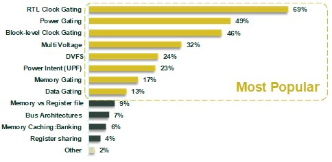
Fig. 2: Usage percentages of known power management techniques (as per Mentor’s 2018 survey)
In this perspective, Dolphin Design is providing a comprehensive set of silicon-proven IP and SW solutions to enable use of all these techniques in a transparent, yet efficient manner.
2) Power Management techniques short review
Power management and low-power techniques can be considered from device-level to SoC-level. Balancing leakage power, dynamic power and area is always achieved by playing with the following formulae:
- Dynamic Power ~W.Vdd² .F
- Leakage Power ~(Vdd/L).e-Vth /S
- Speed ~W/L (Vdd-Vth)²
Standard cell libraries: the foundation of energy-efficient SoC implementation
The design of multi-drive (several W available), multi-Vth (low Vth, regular Vth, high Vth) and multi-length (standard gate length, large gate length) standard cell libraries gave SoC designers the capability to find the right trade-off between speed and power during physical implementation and sign-off ECO loops.
When it comes to achieving the best consumption in sleep and deep-sleep modes, special attention needs to be given to the standard cell libraries that implement the logic functions of the Always-On domain, which is the only part of the SoC that remains active while the rest is dormant. Using high Vth cells is one way to obtain decent figures, however the use of thick oxide transistors is probably the most powerful way to reduce the leakage figures of AON logic by dozens.
Clock gating: let’s stop the clock
At block-level, clock gating was probably one of the first power reduction techniques to be adopted by IC designers. Adding some logic gating on the clock tree reduces the dynamic power by stopping the clock when it’s not needed (we virtually set “F” to 0).

Fig. 3: Clock gating technique
Power Gating: Switch-off what you don’t need
Power gating came next and allowed unused power domains to be switched off, when they are not required by the application, to save leakage (we virtually set “Vdd” to 0). Power gating is generally implemented with a standard Power Management Kit (PMK) that implements a grid- or ring-style structure of power switches. Power switching can significantly reduce the leakage, however the resulting IR-Drop constraint and in-rush current constraint often result in oversized power switch configurations that can break the leakage budget of sleep mode.

Fig. 4: Power gating technique
DVFS, AVS, Body-Biasing
At SoC-level, the need for ultra-low power figures pushed the design community to define more and more complex power states, each block having its own voltage, frequency and power consumption targets. Multi-voltage strategies, among them Near Threshold Voltage (NTV), were the first step, followed by more complex schemes such as dynamic voltage and frequency scaling (DVFS) and adaptive voltage scaling (AVS) that allows a fine-grain control of the SoC performance while reducing the design margins through continuous adjustment of the supply voltage.

Fig. 5: NTV and DVFS, multi-voltage techniques
FD-SOI technologies then introduced a new method to virtually adjust transistors’ threshold voltage by increasing or decreasing the voltage applied on the well.
Techniques such as adaptive body-biasing demonstrate unprecedent power-efficiency numbers, especially when operating at low-voltage, relying on a fully autonomous subsystem that can dynamically adjust the biasing voltages to reach the expected performance.

Fig. 6: Body-biasing technique
PMU: The keystone of SoC power management
The increasing numbers of SoC power modes, created by techniques such as DVFS, require a smart way to set supply voltages and clocks to the right values and make them available in the chip, and to control SoC boot-up and transition from one mode to another.
This is where the Power Management Unit (PMU) comes into the picture.
There is no standard definition of what a PMU can achieve: some applications rely on external Power Management Integrated Circuits (PMIC) to handle voltage regulation, battery charging, power source selection and basic power sequencing, but the need to reduce system costs and the adoption of complex power strategies has pushed ASIC design teams to consider integrating a power management unit (PMU) as a built-in functionality. Foundries now rely on process nodes that enable digital, RF and power management integration on a single die SoC.

Fig. 7: Definition of PMIC and PMU / ePMU
PMU is definitely the keystone of the power management strategy. It drives the boot-up sequence, configures the voltage regulators to get the right output voltage for a given power mode and ensures that power sequencing is properly executed. There are currently two ways to implement a PMU: full custom design or software PMU.
A full custom PMU can achieve ultra-low power figures, especially if it is implemented with low leakage logic cells in the Always-On domain, however it suffers from a lack of configurability and needs to be fully re-designed if there is a change in the SoC architecture or for a product derivative.
A software-based PMU relies on an embedded core, typically a small MCU block, to control power mode sequencing and to manage the interrupts. It can easily be re-configured in-field using conventional firmware updates, however the need to have an MCU that is always active (to control the SoC activity) makes it incompatible with dormant applications that require ultra-low power consumption in hibernation mode.
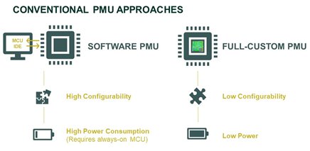
Fig. 8: the pros and cons of conventional PMU approaches
Voltage regulators: from discrete to silicon
The need for reduced BOM costs means that in order to have different supplies available at the same time in the SoC, efficient voltage regulators are increasingly embedded in the SoC, to avoid a proliferation of costly discrete parts on the PCB.
Voltage regulators are basically split in two categories: linear regulators (LDO) and switching regulators (DC-DC converters). Selection depends on application constraints and is often a smart trade-off between efficiency, area and BoM costs.
Today’s IoT SoCs typically embed several linear and switching regulators to supply their main domains (logic, RF, IO, Always-On and analog power).
Leakage current is definitely one of the key analog characteristics that must meet the tight power constraints of IoT systems, but the capability of a DC-DC converter to demonstrate high efficiency, whatever the output current, is a real challenge for analog designers that want to maximize battery autonomy in the end product.
When it comes to achieving ultra-low power figures in sleep and active modes, then the problem moves from high efficiency to low quiescent current, which can generally be achieved using low-quiescent LDOs to supply the Always-On domain.
3) Key Configurations
The previous sections demonstrate that a ULP MCU can be built with many different IP configurations, but it is possible to identify four main categories, which are summarized in the following table.
The first category embeds all products which rely on an external PMIC unit (generally on the PCB) to manage the supply voltage of the MCU.
The second category relates to the MCUs which embark some power management solutions (clock gating and/or regulators for instance) but rely on software constantly running on the MCU to manage the different resources. This configuration presents the advantages of full flexibility with no additional cost of hardware development for the Power Management Unit (PMU) which is virtual.
The third category represents mainstream ULP MCUs for companies which are trying to embed everything (including the PMU as a FSM) so as to squeeze every microwatt out of the chip.
The fourth category shows what can be achieved by SPIDER platform from Dolphin Design. This platform is distinct from the other propositions as it uses specific power gating solutions, unique AON standard cells, ultra-low leakage regulators and a unique adaptive body-bias solution for FD-SOI technologies.
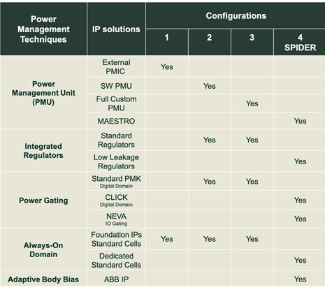
Fig. 9: ULP microcontroller configurations
4) ULPMark Benchmark
Ultra-Low Power (ULP) provides a major design challenge for today’s MCU designers, where product expectations range from running 10 years on a single battery, to harvesting pico-Joules of energy from the environment, to reducing overall global energy demand.
For many years EEMBC has proposed benchmarks that evaluate performance and/or power to enable a fair comparison of microcontrollers and power saving strategies.
There are two benchmarks for ULP microcontrollers, ULPMark-CP (core profile, matching the earlier ULPBench), and ULPMark-PP (peripheral profile).
While the second focuses on architectural improvements in data transfer to and from peripherals, the first one (when cores are equivalent) is really about the technology versus the active power management trade-off. That is the reason why ULPMark-CP is used to evaluate the configurations described in this paper.
ULPMark-CP focuses on the MCU core, in particular the cost of energy during sleep and active modes and the transitions between these two modes. This reference uses a common set of portable workloads on 8-, 16- and 32-bit microcontrollers. The benchmark runs on a 1 second cycle and combines these workloads with an extended period of inactivity (when the microcontroller’s low power modes are used). In other words, the benchmark operates in long periods of sleep mode, followed by a brief wakeup in active mode to perform minimal processing, mimicking a sleepy-edge node conserving energy.
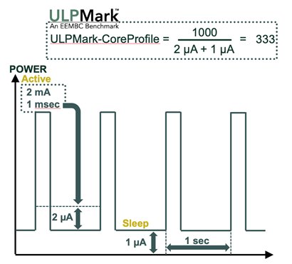
Fig. 10: ULPMark-CP operation
Fig. 10 shows a theoretical example where the active period length lasts for one millisecond (depending on MCU PLL frequency chosen for the benchmark and the required number of cycles to run the benchmark which depends on the MCU architecture). During this 1 ms period, the CPU consumes 2 milliamperes (2 mA), which is effectively 2 microamperes (2 µA) consumption for the 1 second duration of the benchmark. The MCU consumes another 1 microampere in sleep mode.
The ULPMark-CP score calculation is 1000/(active + sleep consumption). In the specific case of Fig. 10, the score is 333 which is a particularly good score.
i) Configuration 1:
In the first configuration, power management is reduced to a minimum. The chip uses an external PMIC to generate its supply voltage in a Go-No-Go fashion. Sleep mode is not used, the chip is simply active or powered down (cf. Fig. 11).
From a SoC design viewpoint, this configuration is the simplest, it translates into a higher BOM on the PCB and no freedom to manage the power.
As a result, this configuration is considered as the worst situation in terms of power and is considered as the reference score for ULPMark-CP, as stated Fig. 17.

Fig. 11: Configuration 1
ii) Configuration 2:
In the second configuration, most of the solutions related to an active power management solution have been implemented in the chip, at the cost of longer design time. This approach requires specialized experts to manage all the different techniques and IPs, and the Unified Power Format.
The primary interest of this approach is to have a sleep mode together with power and clock gating techniques that minimize the power used, especially for the low duty cycle operations that ULP MCUs perform.
Digital domains’ power gating enables a deep-sleep mode. In this mode only a fraction of the chip remains active, to retain some data or to enable wake-up pins, the so-called Always-On domain. This domain is typically made of high-Vt or thick oxide standard cells for their low leakage value typically 0.8 V or 0.9 V depending on the technology. This strategy provides a 62x gain in the ULPMark-CP score compared to configuration 1 (cf Fig. 17).
To achieve this improvement, it is mandatory to permanently run some software that acts as a PMU for the MCU. Even though it can run in very low power mode (for example at 1 MHz), it still consumes power even in sleep modes which reduces the gain by a factor of 4 (cf. Fig. 17).
Finally, running on integrated regulators brings an additional gain in energy efficiency which converts into a 10% gain.
Overall, the ULPMark-CP score is improved by a factor of 16 which is a massive improvement, clarifying why more and more companies are now embedding integrated voltage regulators and active power management.
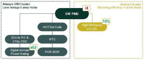
Fig. 12: Configuration 2
iii) Configuration 3:
Although the previous approach has large gains, it incurs a power penalty from the software emulating a PMU for the MCU.
For this reason, the most advanced companies have replaced the SW PMU by a lightweight Finite State Machine (FSM) PMU. This approach greatly reduces the power penalty, bringing a gain factor of 3 on the ULPMark-CP score (cf. Fig. 13).
However, the lack of, or limited reconfigurability of FSMs might be an issue as these MCUs will be used in a large range of applications and situations.
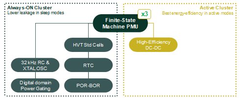
Fig. 13: Configuration 3
iv) Configuration 4:
There is a solution to the trade-off between ultra-low power PMU operations on FSM and high reconfigurability of SW PMU.
Dolphin Design’s embedded Power Controller called MAESTRO is a fully configurable software IP that controls the SoC power management from the start-up sequence to the most advanced DVFS schemes and clock and power gating schemes. This IP presents not only the advantages related to Finite State Machine (ultra-low power and pre-programmed modes) but can also be re-programmed in the field via its drivers offering the same configurability as PMU software running all time on the MCU.
MAESTRO has a comprehensive set of regulators which bring energy efficiency in converting the incoming battery voltage during active modes. All these IPs are also configurable to meet the exact needs and build an optimal supply network while keeping the BOM and integration costs under control. These IPs optimize power consumption during active mode.
Leakage during deep-sleep mode is a major power user for ULP MCUs, so we have developed a unique Always-On set of solutions to enable ultra-low leakage. This set of IPs not only includes ultra-low quiescent LDOs but also dedicated oscillators and power gating solutions.
This configurable FSM-based approach avoids waking-up the MCU.
The software IPs can easily be configured with PowerStudio, a dedicated configuration platform (cf. Fig. 14) which architects an optimized power network supply, while configuring the PMU (cf. Fig. 14). In a second step, the configured RTL is automatically generated with the related verification testbenches and related IP consistency checks for a robust integration (cf. Fig. 15).
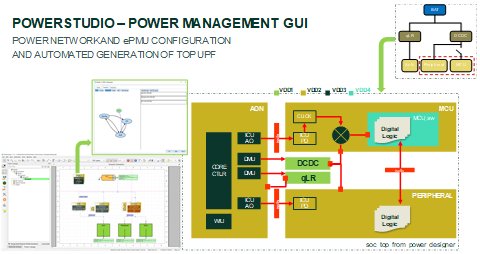
Fig. 14: Dolphin Design PowerStudio GUI

Fig. 15 : Dolphin Design PowerStudio verification and IP consistency checks
As well as PowerStudio, SPIDER from Dolphin Design, offers a coherent set of Ultra-Low Leakage IPs to further enhance the performance by reducing leakage in sleep mode.
The replacement of the standard PMK by Dolphin Design’s solution named CLICK, a tunable power gating solution, offers a 2.2x gain. This gain largely comes from the fact that since the Ron/Roff ratio is tunable in the field, a lower number of switches must be integrated which limits additional leakage in sleep mode.
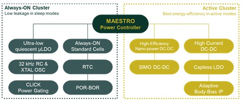
Fig. 16: Dolphin Design IP offering to enable active power management
Another improvement comes from replacing the traditional HVT standard cells by Dolphin Design’s unique AON standard cells which are less leaky though still operate at the same voltage. This provides an additional 1.5x gain.
Finally, the usage of ultra-low leakage linear regulators to supply the Always-On domain results in a 1.1x gain because of the gain in quiescent current (cf. Fig. 16).
Overall, SPIDER offers an additional 3.6x gain in the ULPMark-CP score compared to configuration 3 which represents the most aggressive power management strategy. The gain rises to a tremendous 135x gain compared to a situation where the power is not actively managed (cf. Fig. 17).
5) Results’ summary and benchmarking
Throughout this paper, we have explored how various generic configurations gradually improve an MCU’s power figures. The two main parameters explored were leakage current in sleep mode (in µA) and energy efficiency in active mode (in µA/MHz). These parameters are at the heart of the ULPMark-CoreProfile (CP) score which is widely used to benchmark microcontrollers. Compared to the ULPMark-Peripheral Profile (PP) which is intimately linked to the MCU’s microarchitecture, the ULPMark-CP is almost entirely linked to the power management strategy since most MCUs now use the same CPU (typically a Cortex-M4 or a Cortex-M7).
a) Results’ summary
The improvements in ULPMark-CP scores (relative to configuration 1) are summarized below. The first score line refers to a relative improvement from configuration N-1 to configuration N (ex. 3.6x improvement is observed between configuration 3 and 4). The second score line refers to the absolute improvement since configuration 1 (ex. 135x improvement is observed between configuration 1 and 4).

Fig. 17: ULP MCU configurations ULPMark scores comparison
The largest scores obtained with the usage of Dolphin Design’s SPIDER result from the best-in class IP in the platform. This platform provides other benefits. It was built to provide a strong coherence between the IPs and to enable an easy and robust implementation so as to achieve first-time the most efficient power supply networks with an optimized and silicon proven set of IPs.
b) SPIDER platform overview
This approach is globally explained in Fig. 18. In order to ease the way for power architects, SPIDER platform embeds a GUI called PowerStudio which helps to define, architect and build any kind of power supply network during the specification phase. Figures of Merit (FOM) are automatically computed and can be compared using the FOM Podium features to ensure the best selection for the product. In this phase, not only the regulators and power gating solutions are selected and sized accordingly to the applicative targets, but also the MAESTRO Power Controller is fully configured (including Start-Up sequences and all the preprogrammed transition sequences).
Once the selection is done, the PMU RTL is automatically generated without any human intervention, since the configuration plan performed during the first phase is part of a larger domain where the IP is fully verified.
In the third phase, appropriate IP compatibility checks are run together with automatically generated verification test benches to check the PMU integration in the RTL.
Finally, at runtime, MAESTRO can be reconfigured on-demand via software (drivers are provided). If it is not needed, it runs like a standard FSM on the pre-programmed Start-Up Sequence and Transition Sequences.

Fig. 18: SPIDER Platform at a glance
c) Benchmarking
Since a 3.6x gain compared to the most advanced product configurations might look overoptimistic, we have run some MCUs on silicon (on 40 nm LP and 22FDX technologies) to measure both the leakage current in sleep mode and the energy efficiency in active modes. Experimental results are presented in Fig. 19. The 40LP trial is focused on, with the disclosure of the chip layout because most commercial MCUs today use technologies ranging from 90 nm to 40 nm.
Most renowned MCU companies provide, either on their website or in the application notes, similar measurements for their commercial chips. Fig. 19 summarizes some of these values for a large range of MCUs including both ULP MCUs (with a maximum frequency of 100MHz) and high performance MCUs (with a maximum frequency equal to or greater than 200MHz).
From this benchmark, it is clear that even though we are comparing the same technology node (40 nm) and equivalent cores (Cortex-M4 or M7 or equivalent), SPIDER from Dolphin Design enables more than 3x gain, as stated in Fig. 17.

Fig. 19: SPIDER ower Management Platform gains
6) Conclusion
Leveraging its SPIDER platform, Dolphin Design provides a turnkey solution to speed-up the design of advanced power management solutions, from architecture to implementation, and to achieve ultimate energy-efficiency figures in weeks instead of months.
Dolphin Design brings the most advanced solution to secure the silicon and keep the time-to-market under control, with its combination of a state-of-the-art power management IP portfolio (low-leakage LDO, nano-power high-efficiency DC-DC), a fully configurable and low-power Power Controller IP scalable to any SoC complexity, and the unique PowerStudio system tool that speeds up power architecture exploration and PMU seamless integration.
Focus on your core competencies. Do more with less energy.
ABOUT THE AUTHORs
Souhir Mhira received her PhD in Electrical Engineering in 2018 from Aix-Marseille University for her work on advanced in-situ monitoring to enable ultra-low power ICs and highly reliable microcontrollers for automotive and mission-critical applications. Her work covered all aspects from design specifications to product engineering. She then joined Mentor Graphics to work as Application Engineer in the highly technical Design-For-Test (DFT) world. She recently joined Dolphin Design as Lead Application Engineer, focusing on Power Management IPs platform.
Pierre Gazull graduated in 2006 with a M.Sc. in Electrical Engineering from Ecole Supérieure d’Ingénieurs en Electronique et Electrotechnique in Paris. In 2015, he received an Executive Master’s Degree in Management of Technology and Innovation from Grenoble Ecole de Management. Pierre is in charge of Business Development and Product Marketing for Dolphin Design’s SPIDER platform. Prior to joining Dolphin, he worked for STMicroelectronics for 12 years, successively as an R&D Engineer, Senior Engineer and Senior Technical Lead in the field of digital design flows & methodologies. During this period, Pierre contributed to the development of digital design platforms for established and advanced silicon technology nodes and was involved in key SoC and ASIC projects targeting IoT, automotive, image sensors and MCU markets.
REFERENCES
Related Semiconductor IP
- 6-bit, 12 GSPS Flash ADC - GlobalFoundries 22nm
- LunaNet AFS LDPC Encoder and Decoder IP Core
- ReRAM NVM in DB HiTek 130nm BCD
- UFS 5.0 Host Controller IP
- PDM Receiver/PDM-to-PCM Converter
Related Articles
- Implementing Power Management IP for Dynamic and Static Power Reduction in Configurable Microprocessors using the Galaxy Design Platform at 130nm
- Optimizing System Management in the Platform SoC Era
- Beat power management challenges in advanced LTE smartphones
- Who's managing your power management?
Latest Articles
- A Lightweight High-Throughput Collective-Capable NoC for Large-Scale ML Accelerators
- Quantifying Uncertainty in FMEDA Safety Metrics: An Error Propagation Approach for Enhanced ASIC Verification
- SoK: From Silicon to Netlist and Beyond Two Decades of Hardware Reverse Engineering Research
- An FPGA-Based SoC Architecture with a RISC-V Controller for Energy-Efficient Temporal-Coding Spiking Neural Networks
- Enabling RISC-V Vector Code Generation in MLIR through Custom xDSL Lowerings