Advanced Power Management in Embedded Memory Subsystems
Lisa Minwell, Synopsys
Abstract :
Successful low-power IC designs implement several power management schemes through a comprehensive design, implementation and verification tool chain that understands the power intent. These designs include a large portion of embedded memories that may dominate the chip’s power allocation. Minimizing power while maximizing performance and density are the primary focus for today’s SoC designers that are challenged with the increasing embedded memory count driven by the rich A/V content in today’s consumer products.
This paper will address minimizing low-power design complexity with power, performance and density optimized IP. It will cover the power problem, and the complexity of designing with multiple power domains in SoC designs that contain embedded memory. The paper will include the trade-offs and benefits of various power management features as well as the implementation of the design for superior testability by providing optimal test resource partitioning.
Balancing Market Requirements with Technology Challenges
Today’s markets are demanding power-efficient SoC’s with rich audio/video (A/V) content through a convergence of several markets. Some examples of this include increased content of gaming and multimedia functions driving mobile and handheld hardware performance with long battery life. Increased video content is also driving rapid growth in mobile internet traffic leading the necessity for tera-byte storage drives. At the same time, there is an environmental drive for a green data center and low-power storage.
As processing power of Graphics Processor Units (GPUs) has increased, so has their need for power savings. High performance GPUs consume more energy than current CPUs (Figure 1). However, the goals for these processors with every new generation is to keep the die size constant while the number of transistors increases to boost performance. The content and variety of embedded memory and logic is also increased while the power density is kept constant.
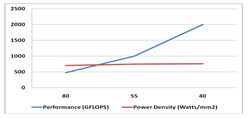
Figure 1 – GPU Power Density
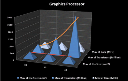
Figure 2 – Graphics Processor
AMD’s (Advanced Micro Device Inc.) Radeon graphics processor HD-4670 has 320 shader processors while the HD-5570 has increased the shader processor count to 400. The number of transistors has also grown from 514 million to 627 million respectively during the migration from 55nm to 40nm process technology.
The technology has kept up with Moore’s Law amazingly well, however, it is not without its own challenges. Both systematic and random variations have increased driving strict Design For Manufacturability (DFM) rules and restricted design rules. As the silicon process migrates at the most advanced technology nodes, the SRAM bitcell area is scaling less than 50% with difficulties in performance scaling, low voltage operation, and increased leakage. The SRAM bitcell is much more sensitive to lowering VDD than standard logic gates because it is a ratioed circuit that depends on the relative strengths of its transistors. As the transistor threshold voltage variation increases in advanced process technologies the SRAM array begins to suffer more failures.
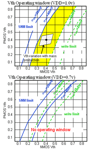
Figure 3 – SRAM Bitcell Static Noise Margin
Figure 3 illustrates the effects of voltage on the static noise margin (SNM). A 40mV sigma provides enough margin to compensate for transistor threshold voltage variation at 1.0V. However, there is no window of operation as the voltage is dropped to 0.7V.
Embedded memory IP architects must navigate these technology challenges while offering increased performance, density, and power management capabilities.
There are several approaches that the embedded memory IP providers may incorporate to mitigate READ and WRITE failures that occur at low voltage operation where the Static Noise Margin is very small. These approaches may include techniques such as Read Assist, Write Assist, and use of Dual Voltage Rails.
Read Assist reduces the influence of the bitline bias thereby stretching the bit cell static noise margin by pulsing the wordline, amplifying the signals on all bitlines, and lowering the bitline pre-charge level. The bitlines will also be architected to be shorter.
Write Assist provides the ability to dynamically control the voltage supplies to the bit cell to compensate for the potential mismatch between pass-gate and pull-up transistors of the bit cell. The bitcell VDD is lowered and the VSS is raised to reduce the strength of the pull-up and increase the drive strength of the pass-gate.
A dual voltage rail architecture provides the separation of the SRAM array from the logic supply voltage. This enables the bit cells to have a stable voltage supply within a safe voltage range for nominal static noise margin. The peripheral logic voltage may be significantly lowered for dynamic power savings. A voltage level shifter is introduced inside the memory to manage the voltage differential between the array and the periphery logic.
Dynamic Power Savings Example with Dual Voltage Rail Implementation
In this example, the historical memory content of Radeon graphics processors was studied over several technology generations. Synopsys DesignWare memories were compiled to comprise the total memory content. This example included High Speed Single Port and Dual Port SRAMs, Ultra-High Density 2-Port Register Files as well as High Density 2-Port Register Files.

Figure 4- Radeon Graphics Processor Example
As shown in Figure 4, the processor core frequency has been increasing with the product generations as they are processed on advanced technologies. The total transistor count has increased significantly from 700 million at 80nm to 4 billion at 28nm. The total memory content has also increased significantly from 82Mb to 534Mb respectively. When calculating the dynamic power contribution of this embedded memory using a representative set of compiled embedded memory instances, the dynamic power contribution for the memory has increased with the increased memory content from 5.21 Watts to 20.36 Watts.
During the operation of the graphics processor, in a mode that requires no processing, the frequency requirements may be significantly lower. This allows the use of dynamic voltage frequency scaling (DVFS). Dynamic frequency is a technique in computer architecture whereby the frequency of a microprocessor is automatically adjusted "on-the-fly", either to conserve power or to reduce the amount of heat generated by the chip. Less heat output reduces the cooling cost of the fan by reducing energy.
Dynamic power is equal to the switching capacitance per clock cycle multiplied by the square of the operating voltage and the switching frequency.
P = C* V2 * F
The frequency scaling in DVFS reduces the number of operations a processor can issue. Therefore, it is used during times when the chip is not CPU bound. The voltage component is the significant contributor to the power savings.
When dual voltage rails are implemented, the SoC designer has the ability to reduce the power supply significantly in the periphery (VDDnominal – 20% or more) while maintaining a safe supply for the memory bit cells (typically equal to or greater than VDDnominal -10%).
This example included the following 28nm compiled embedded memory with dual voltage rails enabled:
- 250 Mb Ultra High Density 2-Port Register Files
- 212 Mb High Density 1 and 2-Port Register Files
- 64 Mb High Speed Single Port SRAM
- 8 Mb High Speed Dual Port SRAM
When the voltage is dropped to VDDnominal – 20% for the periphery and SRAM array voltage is lowered to VDDnominal – 10%, the dynamic power savings is significant. The embedded memory contribution to the graphic processor total dissipated power reduces from 20 Watts to 2.4 Watts. The other contributing factor is the reduction in the frequency from 667MHz to 220MHz (Figure 5).
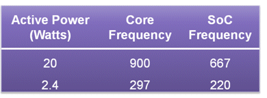
Figure 5 – Dynamic Power Savings with Dual Voltage Rail Implementation at 28nm
Static Power Savings Techniques in Embedded Memory
With the consumer market driving a convergence of features into compact mobile devices, the length of the mobile device’s battery life become a significant deciding factor for the consumer. A quick review of today’s smart phones reveals a range of standby times from 146 hours to 490 hours. However the same devices specify that the maximum battery life ranges from 300 minutes to 420 minutes.
These devices contain a sizable amount of embedded memory with their increased feature set. Many of these devices contain multiple microprocessors and image signal processors (each with embedded caches), graphics accelerators, boot ROM’s, etc. As stated previously, with advanced technologies, the bit cell is more sensitive to a lower voltage (VDD). As shown in Figure 6, the nominal voltage at TSMC has been steadily dropping since 130nm. The bit cell leakage is not scaling the same as the logic transistors. It is increasing relative to logic.
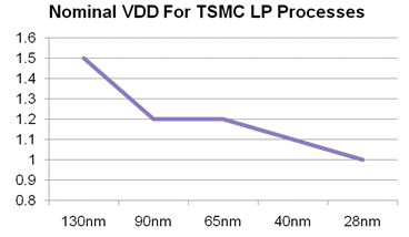
Figure 6 – Nominal VDD for TSMC Low Power Processes
One technique that mitigates the increase in leakage is the use of a high transistor threshold voltage implant. This technique typically trades-off decreased leakage for decreased performance. Another method includes biasing. Biasing is a method of establishing predetermined voltages and/or currents at various points of an electronic circuit to set an appropriate operating point.
One approach is substrate or back biasing. This approach raises the transistor thresholds to reduce leakage. For the PMOS transistors the body of the transistor is biased to a voltage high than VDD. For NMOS transistors, the body of the transistor is biased to a voltage lower than VDD. An advanced techniques that allows the bias to be applied dynamically is referred to as Automatic Body Bias (ABB). This approach has area and routing penalties as well as special logic cell requirements to provide the voltages for the transistor substrate. A substrate-bias generator is required which also consumes more dynamic power.
Another technique of biasing may include a source-biasing mechanism for leakage reduction. This technique provides a standby mode for the SRAM whereby the bit cell’s wordline is deselected and a source-biasing potential is applied to the bit cell. In read mode, the wordline is selected prior to the deactivating the source-biasing potential. Upon completion of reading, the source-biasing potential is re-activated.
Static Power Savings Example with SRAM Biasing and Integrated Power Switches
Embedded memory compilers may offer a compile-time option to enable various power management modes. These modes may include LIGHT SLEEP (LS), DEEP SLEEP (DS), and SHUTDOWN (SD). Each of these modes may be controlled digitally by the assertion/dessertion of a control signal of the memory instance. These modes combine source-biasing for the memory array with the ability to turn off the power supply to the logic devices in the periphery. There is a benefit of significant static power savings while retaining the written contents of the bit cells (retention). There is a small wake-up latency and in-rush current at wake-up because the capacitance is limited with this implementation.
The following example includes the typical embedded memory content for an applications processor in a typical smart phone. It includes a total of 56.56Mb of embedded SRAM with the following architectures:
- 28.56 Mb High Density 1 and 2-Port Register Files
- 4 Mb High Speed 1-Port SRAM Cache
- 20 Mb High Density Single Port SRAM
- 4 Mb High Density Dual Port SRAM
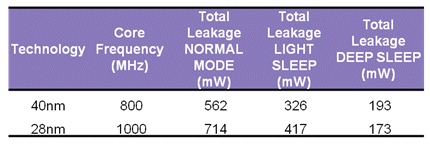
Figure 7 – Application Processor Example Static Power Savings (VDDnominal +10%, 125’C, FF)
The resulting leakage savings with LIGHT SLEEP mode was 42% for both 40nm and 28nm Low Power processes. With the addition of embedded memory periphery power down, the savings increased. The DEEP SLEEP mode provided a 66% to 76% decrease in leakage.
Summary
Today’s consumer electronics markets require optimal performance, high density, low power embedded memories. Advanced process technologies present challenges to SoC designers with increased variation and the lack of bit cell scaling. Two examples provided in this paper demonstrate both dynamic and static power management techniques while meeting the density and performance requirements of graphics and application processors.
Dynamic Voltage Frequency Scaling (DVFS), enabled with dual voltage rails for the embedded memories, resulted in an 85% savings in dynamic power when operating at a lower frequency for non-CPU bound operation.
LIGHT SLEEP and DEEP SLEEP modes were analyzed in an application processor example. These modes provide approximately 42% and 70% standby power savings respectively.
The Synopsys DesignWare Embedded Memory Compilers offer feature-rich power management capabilities for today’s demanding market requirements.
References
- http://www.tomshardware.com/reviews/radeon-hd5570
- Masano Yamaoka, et al, VLSI 2004, Hitachi
- Michael Clinton, ISSCC 2008, Texas Instruments
- J. M. Rabaey. Digital Integrated Circuits. Prentice Hall, 1996
- http://cell-phones.toptenreviews.com
- TSMC 2010 Technology Symposium, April 2010
- Randy Mann et al, “Limits of Bias Based Assist Methods in Nano-Scale 6T SRAM”, University of Virginia
- Stephen Kosonocky et al, “Enhanced Multi-threshold (MTCMOS) Circuits Using Variable Well Bias”, IBM
Related Semiconductor IP
- 6-bit, 12 GSPS Flash ADC - GlobalFoundries 22nm
- LunaNet AFS LDPC Encoder and Decoder IP Core
- ReRAM NVM in DB HiTek 130nm BCD
- UFS 5.0 Host Controller IP
- PDM Receiver/PDM-to-PCM Converter
Related Articles
- Memory solution addressing power and security problems in embedded designs
- Power management in embedded software
- The pivotal role power management IP plays in chip design
- NAND Flash memory in embedded systems
Latest Articles
- A Lightweight High-Throughput Collective-Capable NoC for Large-Scale ML Accelerators
- Quantifying Uncertainty in FMEDA Safety Metrics: An Error Propagation Approach for Enhanced ASIC Verification
- SoK: From Silicon to Netlist and Beyond Two Decades of Hardware Reverse Engineering Research
- An FPGA-Based SoC Architecture with a RISC-V Controller for Energy-Efficient Temporal-Coding Spiking Neural Networks
- Enabling RISC-V Vector Code Generation in MLIR through Custom xDSL Lowerings