Power analysis of clock gating at RTL
By Narayana Koduri, Kiran Vittal, Atrenta Inc. (San Jose, Calif.)
Introduction
In today’s semiconductor designs, lower power consumption is mandatory for mobile and handheld applications for longer battery life and even networking or storage devices for low carbon footprint requirements. Clock power consumes 60-70 percent of total chip power and is expected to significantly increase in the next generation of designs at 45nm and below. This is due to the fact that power is directly proportional to voltage and the frequency of the clock as shown in the following equation:
Power = Capacitance * (Voltage) 2 * (Frequency)
Hence, reducing clock power is very important. Clock gating is a key power reduction technique used by many designers and is typically implemented by gate-level power synthesis tools.
In this article, we will discuss the use of clock gating techniques with design examples for achieving lower power and also highlight the impact of clock gating on different areas of the design process like metastability with clock domain crossings and testability. The article also details the do's and don'ts of clock gating to avoid chip failures and unnecessary power dissipation.
1 HOW TO IMPLEMENT CLOCK GATING
When there is no activity at a register “data” input, there is no need to clock the register and hence the “clock” can be gated to switch it off. If the clock feeds a bank of registers, an “enable” signal can be used to gate the clock, which is called the “clock gating enable”.

Figure 1: RTL Code Examples with Enable
As shown in Figure 1, when an “explicit” clock enable exists in the RTL code, synthesis tools may choose between two possible implementations. The implementation as shown in Figure 1a, is a “re-circulating register” implementation, where the enable is used to either select a new data value or re-circulate the previous data value.
The implementation as shown in Figure 1b is a “gated clock” implementation. When the enable is off, the clock is disabled. The output of the two implementations will always be identical, but the timing and power behavior will be different.
2 HOW TO ANALYZE POWER AT RTL
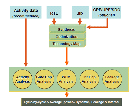
Figure 2: RTL Power Estimation Flow
Early power estimation at RTL can help the designer to quickly explore different architectures like replacing large memories with smaller memories or register files and find power bugs early in the design before it is found too late at the gate-level where synthesis and place and route steps will have to be iterated to meet the required power budget for the design.
Figure 2 illustrates the details of the required and optional inputs to the RTL power estimation flow with Atrenta’s SpyGlass®-Power solution:
- Synthesizable RTL Design – In order to understand the gate count and power characteristics of a design, it must be synthesizable. Portions of the design which are not synthesizable or not finished yet can be represented as black boxes and power data can be provided for these as part of the power library data.
- Power Library Data for the Process – The liberty format has a representation for power data which most library providers use. v Activity Data – In order to estimate power accurately, waveforms for an RTL simulation of the design should be provided in VCD, FSDB, or SAIF format.
- Power Intent – UPF/CPF can be used to define the power intent for estimating the power at RTL.
- Timing Constraints (optional) – There are several Synopsys Design Constraints (SDC) timing constraints which may be useful for power estimation, such as set_case_analysis or set_output_load. An SDC file may be optionally supplied.
3 HOW GOOD ARE EXISTING ENABLES IN THE RTL DESIGN?
It is important to check the effect of clock gating enables to save power in every block of the design. A sample enable scorecard report is shown in Figure 3.
Using the enable scorecard, it is easy to analyze different blocks for clock activity and learn how much more clock gating is possible to reduce the activity. For example, the design unit “mc_cont” in Figure 3 has only 39.88 percent of the registers enabled and there are 96 more new gating opportunities for the design. In the case of design unit “mc_rf”, even though there are 90.66 percent of the registers gated, only 0.6 percent of the clock activity has been saved. This means that clock gating is not very effective on this block. In the latter part of this article, we will discuss how to avoid ineffective clock gates in the design.
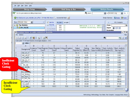
Figure 3: Enable Scorecard Report
In addition to the enable scorecard, it is useful to have a graph for the enable duty cycle over time. Figure 4 shows an example of graph for “Enabled Registers vs. Time” for an RTL design.
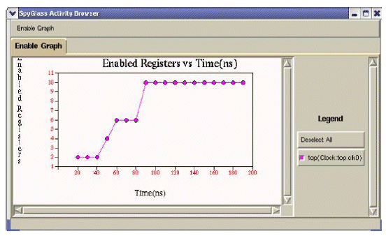
Figure 4: Graph for Enable Duty Cycle vs. Time
The graph in Figure 4 shows that at time 0-40 nanoseconds (ns) only 2 registers are enabled based on the functional simulation data for the particular operational mode. However, between 90-190 ns, 10 registers are enabled. This graph is very helpful in identifying which operational modes have insufficient clock gating, hence resulting in higher than necessary power in the design. Similarly, the activity of the enables can be analyzed for all blocks in the design and at the system-on-chip (SoC) level to improve their performance to switch off the clock for the most number of registers for longer durations.
4 FINDING NEW ENABLES AT RTL
In this section, we will look at an example to analyze the design to find new gating opportunities. In Figure 5, you can see that the “Uxx” registers on the left side are already gated. But downstream registers “Dxx” are still driven by a free running clock. Hence, even though the upstream registers ”Uxx” are not active, there is unnecessary switching of the downstream registers. So, to save this switching power, the enable for upstream registers can be delayed and used to gate the downstream registers without affecting the functionality of the design. Similarly, we can also find additional gating opportunities further upstream to the registers “Uxx”.
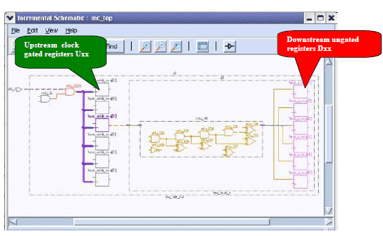
Figure 5: New Clock Gating Opportunities found at RTL
As shown in Figure 6, the designer can identify the downstream and middle register “B” as a gating opportunity by tracing forward from the first register “A”. However, we cannot find a clock gating opportunity for register “C” until the clock gating opportunity for the downstream register “B” has been identified. Hence, an iterative and incremental analysis is needed to find all the clock gating opportunities in the design.
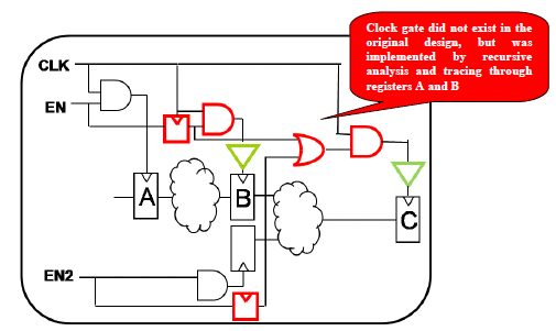
Figure 6: Finding Recursive Levels of Clock Gating Opportunities
Finally, let us look at the design situation in Figure 7. As discussed earlier, we can find a clock gating opportunity for an upstream register. However, at the same time, we can also save power dissipation caused by big operators like multipliers and comparators in between the registers. But this results in the duplication of the enable logic of the downstream register for the upstream register as well. This raises a question - “Does the new enable really save power?”
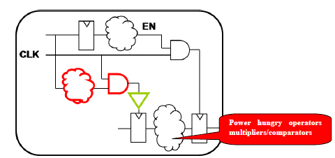
Figure 7: New Enables Saving Data Power
5 DO THE NEW ENABLES REALLY SAVE POWER?
So far, we have discussed identification of new clock gating opportunities in the design. But how do we know if these opportunities actually save power? Before implementing clock gates, it is critical to make sure that all gating opportunities save power instead of increasing power. For example, if the clock enable is always high, inserting a clock gate and additional enable logic will consume more power. In addition to increasing power due to new enables, every time a clock gate is added to the clock tree it introduces an additional delay and makes clock tree synthesis more difficult.
Just performing activity analysis is not enough to see if the new enables actually save power. Differential power computation is actually required to calculate the power savings after gating.
The report in Figure 8 shows the power consumed before and after gating. This helps the designer to choose only those gates that can save power significantly and ignore opportunities that do not save power.
Power hungry operators multipliers/comparators
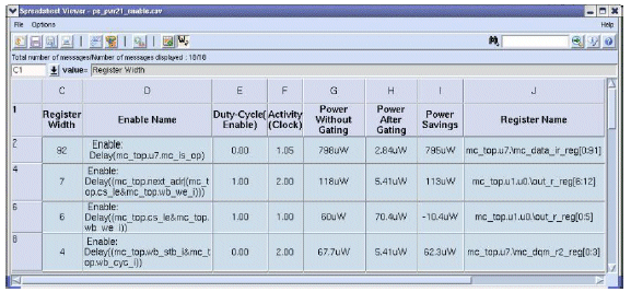
Figure 8: Report for Power Savings for New Enables
6 HOW TO ADD NEW ENABLES TO THE DESIGN
As shown in Figure 9, advanced power reduction tools like SpyGlass-Power can not only find new enable opportunities for the original implementation, but also fix the RTL design automatically. These tools need to support most commonly used RTL languages like VHDL, Verilog and System Verilog for AutoFix. Apart from looking at the comments in the AutoFixed RTL to see the areas of changes, the designer can also review the detailed reports and highlighted schematics to come up with new gating opportunities in the design.
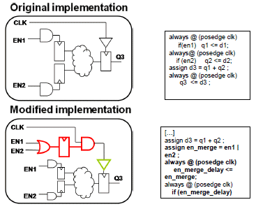
Figure 9: RTL AutoFix for New Enables
But how does the designer know if the new AutoFixed design is functionally equivalent to the original RTL after power reduction changes? The power reduction changes in the new RTL can be verified with simulation or manual review or sequential formal analysis.
If the original RTL and new AutoFixed RTL are run through a standard logic equivalency checking tool, it will report mismatches because equivalence checking tools only check for combinational changes to the design and do not understand sequential changes for new enables introduced for power reduction. In cases where the enable is modified with additional register logic to be made available in the previous clock cycle or delayed, standard combinatorial equivalency checking tools will report a mismatch, even though the circuits are functionally correct.
Hence, the designer has to perform full-blown traditional simulation which takes a long time. Alternatively, the user now has the option to AutoFix the design and validate the new RTL though a sequential equivalence checking (SEC) capability in SpyGlass-Power. This will verify that the functionality of the design is equivalent to the original RTL much faster.
7 HOW TO KNOW IF THE NEW ENABLES DO NOT BREAK THE DESIGN
Designers using automated fixing of RTL for new enables and downstream gate-level clock gating solutions should know if the changes introduce metastability issues on clock domain crossings for asynchronous clocks.
Figure 10 shows a real design scenario where clock gate was introduced by a power optimization tool between two asynchronous clock domains that caused a design re-spin. So, it is very important to use an automated power-reduction solution that is intelligent enough to identify that the new power reduction opportunities are clock domain crossing (CDC) safe.
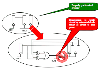
Figure 10: Clock Gating Causing CDC Problems
8 HOW TO CONTROL SYNTHESIS TOOLS TO IMPLEMENT ENABLES EFFICIENTLY
All the traditional synthesis tools implement clock gating based on register bit-width. Power synthesis implements a clock gate if the register bit-width is equal to or more than the one specified by the user. We have already discussed how downstream clock gating may introduce CDC issues. However, these clock gates may also result in additional power dissipation rather than savings. This is due to the fact that synthesis tools may also implement bad clock gating enables.
In Figure 11, the number of clock enables that can be implemented through the synthesis tool versus register bit-width is plotted as a scatter plot. Typically, the register width threshold is chosen as 4 or 8, and is shown as a line on the scatter plot. That means clock gating enables lesser than the register width are not being implemented and also the clock gating enables shown below the x-axis in red color are being implemented. So, the designer is missing some real power saving opportunities that are shown to the left of the register bit-width threshold and also implementing negative power savings as shown in the red color.
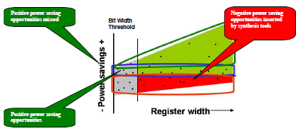
Figure 11: Power Savings for Clock Gating with Synthesis
Hence, the designer needs to analyze each and every clock gating enable that can save power and discard the opportunities that consume more power. To do this, we need to evaluate the duty cycle of the enable, data at the register input and width of the register. Hence, it is very important to calculate the power savings and estimate whether registers with re-circulation multiplexers dissipate more power than the clock-gated registers.
SpyGlass-Power can calculate the effect of enables on power savings instead of just register width as shown in Figure 12. It can also generate a “don’t touch” script for negative power opportunities, which the designer can use with the synthesis tool and discard the registers that dissipate more power with clock gating. Avoiding unnecessary clock gates will not only reduce power but also make clock tree synthesis easier. In Figure 12, the registers listed at the top save power and some of the registers have diminished savings and at the bottom, while some registers are shown dissipating more power.
The designer definitely needs to avoid synthesis tools implementing clock gates for the registers which dissipate more power. The designer need not be concerned about the bit-width threshold, as the tool will analyze the bad clock gates and help to not insert them during synthesis.
Positive power saving opportunities missed
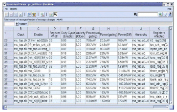
Figure 12: Power Savings Report Due to Clock Gating
9 DO THE TEST CLOCKS PROPAGATE CORRECTLY THROUGH CLOCK GATING?
For a design with instantiated integrated clock gating (ICG) cells to save power, the designer also needs to perform checks to make sure that test clocks are propagated correctly through various modes such as scan shift, capture and at-speed capture to avoid finding issues later after synthesis, during scan insertion or test pattern generation.
It is equally important to validate the RTL with instantiated integrated clock gating cells (ICGC) and verify that the design is clean in the respective test modes. The checks should mainly constitute:
- Clock enable should be controllable to “ON/OFF” state in at-speed, capture, shift modes
- Enable signal reaching the clock gating cell should be observable in at-speed and capture modes
Figure 13 illustrates some of this analysis.
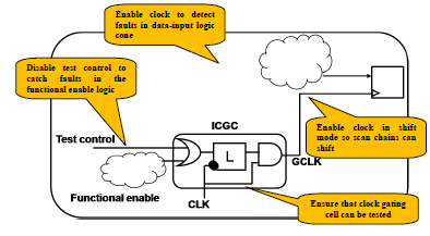
Figure 13: Clock Gating and Testability Analysis
10 SUMMARY
This article discusses a solution for clock gating analysis and implementation at RTL for power reduction. The RTL approach is important because designers usually verify power only at the gate level and any change to the RTL needs many design iterations to reduce power. The RTL solution thus saves weeks of effort by fixing potential power issues up-front.
It is important to have a tool for accurate RTL power estimation and power reduction by automatically and efficiently implementing new clock enables and verifying that the new RTL is CDC-safe and is functionally verified with sequential formal analysis.
It is equally important to verify that the clock gating for power does not affect the overall functionality by creating new clock domain crossing issues or impacts the testability of the design as well.
About the authors:
 Narayana Koduri is a senior corporate applications engineer for the SpyGlass-Power product line at Atrenta Inc and has been supporting semi-conductor designers in the areas of RTL power estimation, reduction and verification for the past 6 years. He has 9 years experience in EDA and chip design. Prior to joining Atrenta, he held an application/design engineer position at Trident Techlabs, India. Narayana Koduri holds a bachelor degree in engineering from Anna University, India.
 Kiran Vittal is a Product Marketing Director at Atrenta, with 19 years of experience in EDA and semiconductor design. Prior to joining Atrenta, he held engineering, field applications and product marketing positions at Synopsys Inc, ViewLogic Inc and Mentor Graphics Inc. Vittal holds an MBA from Santa Clara University and a bachelor's degree in electronics engineering from India.
Related Semiconductor IP
- NPU IP Core for Mobile
- NPU IP Core for Edge
- Specialized Video Processing NPU IP
- HYPERBUS™ Memory Controller
- AV1 Video Encoder IP
Related White Papers
- Sequential clock gating maximizes power savings at IP level
- Context Based Clock Gating Technique For Low Power Designs of IoT Applications - A DesignWare IP Case Study
- Achieving Low power with Active Clock Gating for IoT in IPs
- Throttle IP Core Power Dissipation: Use RTL Power Analysis Early and Often
Latest White Papers
- Ramping Up Open-Source RISC-V Cores: Assessing the Energy Efficiency of Superscalar, Out-of-Order Execution
- Transition Fixes in 3nm Multi-Voltage SoC Design
- CXL Topology-Aware and Expander-Driven Prefetching: Unlocking SSD Performance
- Breaking the Memory Bandwidth Boundary. GDDR7 IP Design Challenges & Solutions
- Automating NoC Design to Tackle Rising SoC Complexity