Pipeline vs. Sigma Delta ADC for Communications Applications
By Noel O'Riordan, Mixed-Signal IP Group, Silicon & Software Systems (S3)
Introduction
The Analog-to-Digital Converter (ADC) is a key component in digital communications receive channels, and the correct choice of ADC is critical for optimizing system design. In this article, we discuss what design factors drive the selection of the ADC, how to specify the ADC and when to choose between a Pipeline ADC and a Sigma-Delta (Σ/Δ) ADC.
1 ADC
Two of the most popular ADC architectures today are the Pipeline ADC and the Sigma Delta ADC. Traditionally each has had its own distinct application areas, and interestingly, nowadays, there are some areas where both can be applied. We will look at this and determine how to make the appropriate ADC choice.
1.1 ADC Basics
To correctly convert a continuous analog signal to its discrete digital representation, the ADC sampling frequency (or sampling rate in MS/s) must be twice the bandwidth of the signal. In practice the input signal’s bandwidth must be limited by an analog ‘Anti-Aliasing’ filter, and the minimum ADC sampling frequency is referred to as the ‘Nyquist frequency’.
As we will see, the ADC is often operated at a higher sampling rate to relax the filtering requirements, and the Over-Sampling Ratio (OSR) is the number of times the actual sampling rate is greater than the minimum Nyquist frequency.
Converting a continuous analog signal into a discrete digital code, involves unavoidable errors due to quantisation noise, device noise and circuit non-idealities. The number of bits for the ADC is dependent on the Signal-to-Noise-and-Distortion Ratio (SNDR) required in the digital modem decoder. Accurate determination of the SNDR specification is vital for selecting the best ADC: if it is over-dimensioned, the power and area of the ADC will increase rapidly. Another related key ADC specification is the Effective Number of Bits (ENOB), being the achievable dynamic resolution of the ADC.
1.2 Pipeline ADC
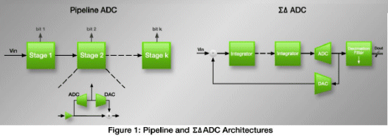
A Pipeline ADC consists of a cascade of stages, each of which contains a low resolution ADC, DAC and amplifier, that successively convert the analog input into its digital representation, while processing the data in a pipe-lined manner.
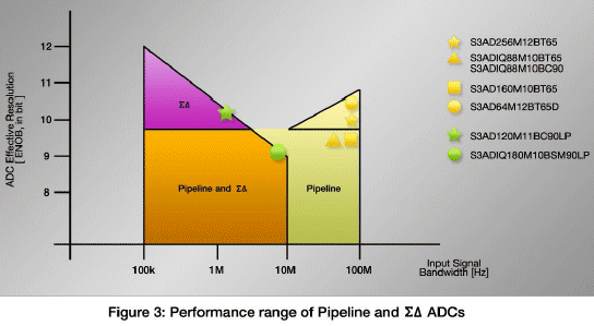
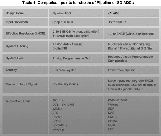
Pipeline ADCs are commonly used for power-efficient high-speed conversion of wide bandwidth input signals (e.g. 10 to 100 MHz). The ADC sampling frequency is usually the Nyquist frequency or lower using small OSRs (e.g. 2 or 4) and the ADC output code resolution is typically between 8 and 14-bit.
The pipeline ADC is an open-loop architecture, having a small inherent latency (e.g. 4 to 6 clock cycles), and a direct relationship between the input signal and the output code.
Pipeline ADCs are typically implemented in CMOS processes using Switched Capacitor (SC) discrete-time circuitry. A Pipeline ADC needs a non-trivial analog Anti-Aliasing filter, which consumes additional power and area.

1.3 Sigma-Delta (Σ/Δ) ADC
Sigma-Delta (Σ/Δ) ADCs are significantly different from pipeline ADCs and some of the conventional specifications should not be applied directly. They are capable of achieving high ENOB/SNDR (e.g. 10 to 12 ENOB and above), for low to medium input signal bandwidths (e.g. 100kHz to 10MHz).
The Sigma-Delta (Σ/Δ) architecture employs feedback from the digital to the analog domain and relies on a high OSR (e.g. 10 to 128). The high oversampling ratio allows very simple analog anti-aliasing filters to be used, saving system power and area, but do require some extra digital filtering. As a result of the feedback, the Sigma-Delta (Σ/Δ) ADC can become unstable for large input signals, and lose performance – so some sort of overload diagnostics are necessary. In addition, there is no direct relationship between the input signal and the digital output code, so dynamic linearity specifications like Spurious Free Dynamic Range (SFDR) are often used instead of Differential and Integral Non- Linearity (DNL/INL).
Sigma-Delta (Σ/Δ) ADCs can be implemented as Discrete-Time (DT) or Continuous-Time (CT) circuits. Discrete- Time Switched-Capacitor Sigma-Delta (Σ/Δ) ADCs are easily programmable for different bandwidths, do not require calibration and are relatively insensitive to clock jitter (which can degrade performance). We will focus on DT SC Sigma-Delta (Σ/Δ) ADCs in this discussion.
2 Receive Path Design
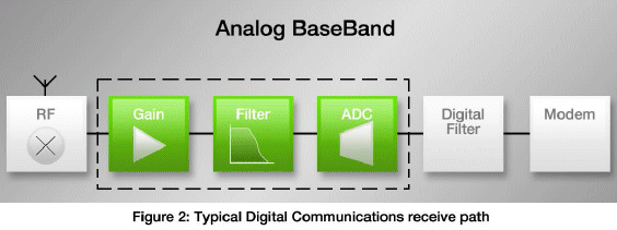
A typical receive path used in digital communications systems is shown below.

The Analog BaseBand (ABB) is of interest here. Gain is required to amplify the signal. Filtering is required to provide anti-aliasing, by band-limiting the signal presented to the ADC, in order to reduce noise and attenuate interference signals (especially important in wireless applications). In designing such a system, the goal is to trade-off gain, noise linearity, under the constraints of minimising power and die area.
The gain and filtering can be distributed at different points in the receive path. Note that digital communication paths are conveniently implemented by splitting the signal into two components, commonly termed I and Q. For baseband applications, such as wireline communications this can be handled in the digital modem and so only one receive path (and ADC) is needed. For wireless applications, such as WLAN/WiMAX/LTE, the RF down-conversion results in the need for two receive paths and two ADCs, often termed IQ ADC. In the digital domain, some form of decimation filter is typically used, to change the sampling rate down to the Nyquist frequency, irrespective of whether a Sigma-Delta (Σ/Δ) or a Pipeline ADC is chosen.
3 Specifying the ADC
Based on the application’s standard, the ENOB/SNDR required for the ADC can be calculated. Filtering plays a large role in determining the ADC ENOB. For example, in wireless applications, often one half of the ADC ENOB figure is needed to handle interference signals that may be present. We will consider three applications: 1) wideband wireline,2) wireless broadband and 3) high-resolution narrow bandwidth wireless.
3.1 Wideband Wireline
Examples of such applications are Powerline Communications and Cable Modem. The bandwidth is of the order of 40MHz to 100MHz and ENOB required varies from 9.0 to above 10 ENOB. The Pipeline ADC is ideally suited for these applications.
For 9 ENOB and slightly above, a 10-bit Pipeline ADC operating from 8 to 80MS/s can be employed, featuring an area of 0.3mm2 while dissipating less than 20mW [1]. For 10 ENOB and above, a 12-bit Pipeline ADC operating at 64MS/s is recommended, typically featuring 0.6mm2 and 60mW [2].
Special consideration should also be given to the fact that the input signal is a composite multitone OFDM signal and not a simple sine-wave, as has traditionally been used to specify ADCs. The multi-tone nature of OFDM signals means this signal is in fact composed by a multitude of low-amplitude sinewaves and this has a major impact for example in relaxing the required sampling clock jitter.
Needlessly specifying too high an ENOB for the ADC will result in extra complexity and cost. High ENOBs with sampling rates greater than 100MS/s (e.g. 256MS/s) can be supported with an Interleaved Pipeline approach [3].
3.2 BroadBand Wireless
Here we will examine two different input signal bandwidths: 4MHz (mobile TV) and 10MHz (LTE). An IQ ADC is used for the two baseband paths after Zero-IF RF down-conversion.
Typical solutions for mobile TV (4MHz) are a 9 ENOB Pipeline ADC operating at OSR of 4 (e.g. 32MS/s sampling rate for the 4MHz bandwidth) or a 10 ENOB Sigma-Delta (Σ/Δ) ADC with an OSR of 15 (e.g. 120MS/s sampling rate for the 4MHz bandwidth). Good examples of Pipeline and Sigma-Delta (Σ/Δ) ADCs [4, 5] show similar areas (0.65mm2) but the pipeline solution features less than half the power (15mW versus 37mW) mainly due to the lower ENOB of 9 versus 10 for the Sigma-Delta (Σ/Δ) ADC. So the architecture choice here is based mainly on system level architecture. The Sigma-Delta (Σ/Δ) ADC allows the order of the analog anti-aliasing filter to be reduced by 3, saving up to 1.0mm2 and 10mW. A digital decimating filter is needed for both types of ADCs, with the Sigma-Delta (Σ/Δ) needing an extra digital filtering stage that consumes 1mW, but negligible area. Both ADCs need a buffer before them to drive the sampling capacitor, and in the case of a Sigma-Delta (Σ/Δ) ADC additional anti-aliasing filtering can be easily incorporated into this buffer at little cost. In this instance, the Sigma-Delta (Σ/Δ) ADC can provide a lower area receive path solution.
For a 10MHz input bandwidth, a typical implementation uses a 9 ENOB IQ Pipeline ADC sampling at 80MS/s (OSR=4) and consuming 40mW [4], or a Sigma-Delta (Σ/Δ) ADC with similar ENOB performance sampling at 180MS/s (OSR=9) and consuming 45mW [6]. In this case, the choice depends more on the customer preference and the possible need for compatibility with higher bandwidths in the future, which might tend to favour a Pipeline ADC.
For higher ENOBs at 10MHz input bandwidth and above, for example 10.5 ENOB as often required in LTE, a 12-bit Pipeline Dual Input IQ ADC sampling each channel at 32MS/s seems to be a good solution, featuring 58mW and 0.65mm2 for the complete IQ solution [7].
3.3 NarrowBand Wireless
High resolutions of 11-12 ENOB are required in bandwidths of a few hundred kHz for standards like GSM. In order to achieve such high performance levels, a Pipeline ADC will require calibration, whereas a Sigma-Delta (Σ/Δ) IQ ADC can provide this resolution while consuming only 7.5mW [8].
For multi standard receivers, such as Software Defined Radio, a Sigma-Delta (Σ/Δ) ADC is the favoured architecture, due to its ease of programmability over a wide range of ENOB/SNDR requirements.
4 Conclusion
Choosing the correct ADC is a crucial step in designing the optimum receive path, and attention must be paid to accurately specifying the ADC by taking the full system into consideration. The information provided in this article should prove useful in making this selection.
S3 provide a comprehensive offering of high performance, low power, silicon proven ADCs for Pipeline and Sigma-Delta (Σ/Δ) architectures covering input bandwidths from 100kHz to 100MHz, in advanced deep sub micron technologies (40nm, 65nm, 90nm, 130nm, 0.180um) and in multiple foundry processes.


S3 Mixed-Signal IP Parts Quoted in this Article:
- [1] S3AD88M10BC90
- [2] S3AD64M12BT65D
- [3] S3AD256M12BT65
- [4] S3ADIQ88M10BC90
- [5] S3AD120M11BC90
- [6] S3ADIQ180M10BSM90LP
- [7] S3AD64MD12BT65D
- [8] S3ADIQ160MSDC13
Related Semiconductor IP
- ADC
- 11 Bit 100 kS/s Ultra-Low Power SAR ADC on GlobalFoundries 22FDSOI
- Ultra-Low-Power 6-13 Bit 1-10 kS/s 1.9 µW SAR ADC on XFAB XT018
- 7 Bit 6 GS/s Folding ADC on Fujitsu 55 nm CS250L
- 12-bit 2GSPS Time Interleaved ADC
Related White Papers
- Understanding sigma delta ADCs: A non-mathematical approach
- Design trade-offs of using SAR and Sigma Delta Converters for Multiplexed Data Acquisition Systems
- Systel Level Design Automation of Pipelined ADC
- Three ways of looking at a sigma-delta ADC device
Latest White Papers
- Boosting RISC-V SoC performance for AI and ML applications
- e-GPU: An Open-Source and Configurable RISC-V Graphic Processing Unit for TinyAI Applications
- How to design secure SoCs, Part II: Key Management
- Seven Key Advantages of Implementing eFPGA with Soft IP vs. Hard IP
- Hardware vs. Software Implementation of Warp-Level Features in Vortex RISC-V GPU