Pushing the Frontier in Managing Power in Embedded ASIC or SoC Design with PCI Express
Santa Clara, CA, USA
Abstract
:
PCI Express is architected to not only meet the demand of high-bandwidth, robustness and reliability of today’s system connectivity, but also to address one of the most critical areas in the embedded ASIC or SoC designs which is to manage power and to reduce power consumption. This paper will discuss some techniques applicable to PCI Express such as changing device power states in coordination with operating system, managing clocks and managing device drivers. In addition, this presentation will present a trade-off analysis between latency and clock frequency with respect to power consumption. The paper will present the PCI Express link power management in details. Moreover, some power-related guidelines such as power well isolation will be suggested for the system designer integrating PCI Express into embedded ASIC or SoC designs.
With increasing speed and increasing number of gates going into silicon due to smaller process geometry, power consumption is on the rise, and could be limiting for many applications. Hence to manage power and reduce power consumption has been a very important aspect of today’s system design. This even becomes more acute in embedded systems which are typically used in mobile and hand-held applications where any amount of extra battery life is welcome. In a typical embedded SoC, we find an on-chip local processor (ARM, MIPS, ARC, or DSP for example) with multiple clock domains and resets. In these applications power savings are tackled from many angles –Logical, Physical, Functional and System. On the logical front many low-power design techniques are followed, and on the physical front many state-of-the-art tools help reduce power consumption on the net list level. This paper is going to focus on power management(PM) achieved through PCI Express on the functional and system level.
To tackle this important issue lets understand the basics of power consumptions first. Then we would discuss how power management is done in a local as well as global level, and how PCI express is addressing this through its innovative link-level power management features. There are three main factors that affect power consumption or dissipation – frequency, operating voltage and switching/node capacitance value as given in the following formula (Power = Kfcv2).
As it can be observed from the equation above, the biggest contributor of power dissipation is voltage. It is proportional to the square of the voltage. PCI Express operates at Smaller Operating Voltage of 1.2V which is much smaller than 5.5/3.3V, the operating voltage for conventional PCI. The other approach to reduce power dissipation is to have Separate Power (Voltage) Wells. The majority portions of the chip can operate in core power supply, and a smaller portion can be used to wake up the rest of the chip, and can be operated on an auxiliary power supply. When the chip is in a sleep mode without the need of doing any useful work, the power supply to the core logic can be turned off, and only a relatively smaller portion of the chip can be still be powered on with the auxiliary supply. This can result in significant average power savings. Later, how this technique applies to PCI Express and the techniques how to do separate power wells in a chip is discussed.
The next big contributor for power consumption is operating frequency. With demand for higher bandwidth, the speed/frequency is on the rise. However PCI Express offers a provision in which the core logic can operate at Reduced Frequency without compromising the throughput. PCI Express defines an interface between the core logic and the physical PHY called the PIPE interface. The PIPE can be operated at 8bit/250MHz (single PIPE) or at 16-bit/125MHz (dual PIPE). With dual PIPE, the core logic can operate at half the clock rate providing same throughput but lower power consumption. There are of course pros and cons of operating at lower frequency and wider data path. The cons are relatively larger latency to process packets with lower frequency. For mobile applications power savings is more important than the extra latency. In other applications such as inter-chip communications, latency may be more important than the power savings, and these applications would opt for single-pipe mode.
Another usage of clock manipulation to achieve power savings is through Clock-gating which is to cut off the clock to portions of logic at times. PCI Express offers many such scopes for clock gating at local as well as broader level. Among these is the CLKREQ# protocol which allows the reference clock from the platform to be turned off. This in turn causes the PLL in the PHY to be turned off, and the clock to the core logic to be turned off. Other techniques to turn off clock inside the PCI Express core logic during some of the Link states are also discussed later sections.
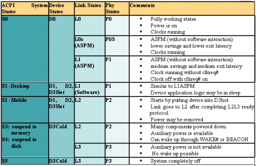
Next, let’s discuss power management from system perspective, describe the basics of it, and how these apply to PCI Express. In a system, power management is a coordinated effort among many components such as Operating System (OS), PM driver, device driver, platform clock/power manager, chipset and device. Advanced Configuration and Power Interface (ACPI) specification defines ACPI System States (S0, S1, S2, S3, S4 and S5) to manage power at the highest level that involves the entire platform and affects many components. S0 is the fully operational state with full power and S5 is the state when the system is completely powered down. As we move from S0 towards S5, more power saving is achieved. The next level in power management is the Device States (D0, D1, D2, D3) defined by PCI PM specification. D0 is fully operational power state with full power on, and D3 is state with most power savings. The lowest level of PM is the PCI Express Link Power States (L0, L0s, L1, L2 and L3). L0 is the fully operational power state with full power on and all clocks running. L3 is the least power consuming state with all power and clock shut off. As we move from L0 towards L3, more power saving is achieved but it comes with larger exit latency from these states to go back to L0 state. The PCI Express PIPE spec also defines PHY P states (P0, P0s, P1, P2, and P3) which are very much analogous to the link states. The table below describes the relationship among the System, Device, Link and Phy states.
Table-1

This section describes the PCI Express Link States in details. The Link states are L0, L0s, L1, L2 and L3, where L0 is fully functional states with full power on, and all the clocks running. L0s is a low exit-latency and relatively lower power saving link state. It is designed to exploit smaller periods of inactivity on the link. L1 offers larger power savings with larger exit latency, and is designed to work on larger period of inactivity on the link. L2 power state gives the most power savings, but it comes with largest exit latency. The exit latency for L0s is in the order of ns (several hundred ns). The exit latency for L1 is in the order of us, and the exit latency for L2 is in the order of ms.
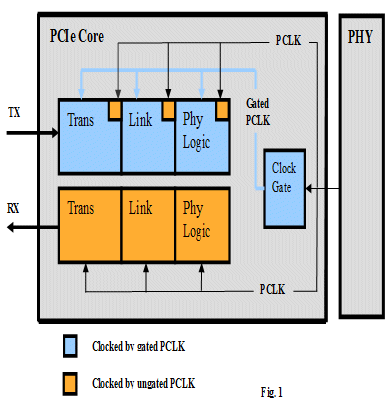
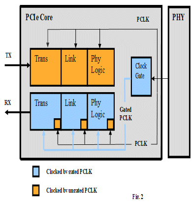
PCI Express L0S link state is comprised of two independent states L0sTX and L0sRX states. The PCI Express link operates on full-duplex mode where data transmission takes places in both directions. The transmit and receive paths are independent of each other which means either the transmit or receive path can be turned off, or both the transmit and receive paths can be turned off. L0sTX deals with the transmit path, and L0sRX deals with the receive path. L0sTX is initiated when the user application has no packet to send. The core logic maintains a timer with a maximum value of 7 us. When the timer expires, the transmit side sends an EIOS (Electrical Idle Ordered State - a type of data link layer packet) and brings the TX+ and TX- lines to common mode voltage. The core logic can make the timer programmable that the device driver can control instead of hard-coding the timer value during synthesis time. This provides finer granularity and can be varied based on traffic patterns and traffic conditions. L0sRX is entered when the link receives EIOS from the device on the other side of the link. Both L0sTX and L0sRX are done at the link level without any knowledge of the OS or PM driver. During L0Stx, certain portions of the PCI core logic (TX layers) can be clock gated, and similarly during L0sRX, certain portions of the PCI core logic (RX layers) can be clock gated as conceptually captured in the diagram below.


PCI Express L1 Link State is divided into two types of L1 states –L1 ASPM and L1-Software initiated. L1 ASPM is fully autonomous mechanism between the two components at the end of a link, and doesn’t involve any software interaction. When the Link enters into L0s (both L0sTX and l0sRX) and stays there for certain period of time, the link power state can be elevated to L1ASPM state. The entry to L1 is always initiated by the PCIe endpoint (device away from the root in the hierarchy), and upstream component (root or switch port) can accept or reject the request to enter L1. When the up component rejects the request, the endpoint has to wait for a minimum period of 10us before it can request again. The wait is there to separate a new request from the previous rejected request. When accepted, both sides send EIOS ordered sets, and enter into electrical idle conditions on the TX lines. The exit from L1 to L0 can be initiated by either side when it has a need to send a packet.
L1-soft is done through software. When software programs the device to enter to non-D0 state which is D1, D2, D3Hot, the PCI Express link enters into L1 state. The mechanism to enter L1 is similar to L1ASPM, but there is no rejection for the software initiated L1. The most commonly used state is D3Hot state where the device application logic also enters into sleep-mode state with most of the functionality being tuned off. PCI Express also provides clock-gating protocol called CLKREQ# which works on top of L1. After the link enters into L1 state, the endpoint can initiate CLKREQ# protocol. The reference clock that is supplied from the platform, and feeds the device, is turned off. This gives additional power savings as PLL inside the PHY is tuned off, and clock to the PCIe core logic is turned off. Another clock gating approach that can be implemented is to self clock gate the PCIe core logic as some platform may opt to keep the reference clock running.
The highest level of power savings through the Link states is L2 State. The software initiates the process to switch off core power in which the up component sends PME_TURN_OFF message to the endpoint. The PME_TURN_OFF message can come when the device is D3Hot state or any time, not necessarily in D3Hot state. When the endpoint receives the PME_TURN_OFF message, it readies itself for eventual power removal, and completes the process by sending acknowledgement. When the process completes, the core power can be turned off. If the system provides an auxiliary power supply or the device has it own auxiliary power supply, the link enters into L2 state, where the core power is turned off. A smaller portion of the logic, powered by auxiliary power, maintains the house-keeping and wake-up logic. When the application wants send packet, it first needs to wake up the system to get back power and clock. PCI express provides two methods for wake up - the traditional side-band WAKE# signal or the in-band Beacon signal. Beacon is very low-frequency (KHz range) sent by the endpoint to the up component. After the system restores the core power supply and clock, the endpoint sends PME message which is similar in concept to the conventional PCI PME#, but it goes out as a message, in stead of being a side-band signal. The next section describes how separate power wells are implemented.
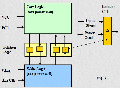
When there are separate power wells (domains) in a chip, Proper Isolation need to be done at the boundary between the logic in these domains. When a power supply to a domain is turned off, the signals going to the powered-on domain from the powered-off domain are floating, and this can cause large leakage current. To address the leakage issue, the signals go through isolating cells which are logical AND gates. One leg of the AND gate is powergood signal that is fed from the powered-on domain, and provides a value of ‘0’. The ‘0’ value for the powergood signal makes the output a deterministic ‘0’ instead of floating value. Isolation is done for signals crossing the power domains in both directions. The following diagram provides picture of how this is done.

In summary, power management is very important part of today’s embedded ASIC and SoC design. PCI Express is being used in many embedded applications where it provides not only the high bandwidth, but also many tools to manage power at different levels. The paper provides how PCIe PM is done at system, device and link level, and how frequency/datapath width trade-off can be applied for certain applications. It provides suggestion for aggressive clock-gating during link states. It also provides ways to make certain inactivity timer to make user-programmable so that device driver can fine tune these values depending on traffic conditions.
Kishore Mishra is the President and CEO of ASIC Architect, Inc that specializes in high-speed interface controllers. His primary focus is on PCI Express, PC Architecture and Power Management. Kishore Mishra holds BSEE degree from NIT Rourkela, India, and MSEE from UT, Toledo, USA. He has 18+ years experience in electronics industry in computer architecture, product development and management. Prior to co-founding ASIC Architect Inc., he held senior engineering and management positions at Intel, Texas Instruments and start-up companies in Silicon Valley. Kishore Mishra holds several patents in the area of computer architecture.
C. C. Hung is the senior product line manager for PCI Express IP core product line at Mentor Graphics. In addition to C. C.’s more than 15 years of experience with embedded hardware and software in consumer electronics, wireless, telecom, and datacom areas, he has served in a variety of senior positions in product management and applications engineering fields with Freescale, Inc., and holds numerous patents and awards. C. C. has an MS in Electrical and Computer Engineering from University of Texas at Austin, an MS in Mechanical Engineering from Penn State University, and a BS from the National Central University in Taiwan.
Related Semiconductor IP
- PCIe - PCI Express Controller
- Scalable Switch Intel® FPGA IP for PCI Express
- Multichannel DMA Intel FPGA IP for PCI Express*
- PCI Express Gen5 SERDES PHY on Samsung 8LPP
- PCI Express Gen4 SERDES PHY on Samsung 7LPP
Related White Papers
- How HyperTransport and PCI Express complement each other
- Advanced switching boosts PCI Express
- Compatibility issue slows PCI Express
- With StarFabric as an on-ramp, the PCI Express Advanced Switching is ready
Latest White Papers
- Boosting RISC-V SoC performance for AI and ML applications
- e-GPU: An Open-Source and Configurable RISC-V Graphic Processing Unit for TinyAI Applications
- How to design secure SoCs, Part II: Key Management
- Seven Key Advantages of Implementing eFPGA with Soft IP vs. Hard IP
- Hardware vs. Software Implementation of Warp-Level Features in Vortex RISC-V GPU