Learning Not to Fear PCI Express Compliance Using a Predictable, Metrics Based Verification Closure Methodology
Mike Bartley, Jim Hutchinson, ClearSpeed Technology Plc
Dimitry Pavlovsky, Pete Heller, Cadence Design Systems
Introduction
On the way to taping out its first PCI Express based SOC, ClearSpeed came face-to-face with the many difficulties of ensuring PCI Express protocol compliance within time and budget constraints. PCI Express is a complex protocol with an extremely large coverage space. From a management perspective, there is simply not an alternative but to apply a metrics-driven verification process to ensure protocol compliance. Unfortunately, even with thousands of tests covering the relevant scenarios, significant coverage holes remain, making this approach unpredictable and costly. The alternative, a general random test approach, isn’t sufficiently predictable.
ClearSpeed has come to realize that the ideal approach yields significant benefits: it minimizes engineering effort while maximizing test deployment control. ClearSpeed got a head-start by using commercial PCIe Verification IP supplied by Cadence. The VIP, called a UVC, includes the Compliance Management System (CMS) which partitions and maps the coverage space to the PCIe specification. CMS also provides a compliance test suite in the form of constrained-random tests (called sequences) to automatically achieve high functional coverage for each PCIe specification section. ClearSpeed then built its own constrained random test suite on top of the UVC’s. Associated coverage is analyzed after each test group run, resulting in clear understanding of where coverage holes lie and guiding where new tests must be directed to reach uncovered scenarios. This approach also has provided ClearSpeed with an invaluable project management tool since it helps them to understand and report on verification status. ClearSpeed now regularly tracks coverage, bug statistics, and test failures in each of the main specification areas.
The methodology, tools used, and implementation guidelines employed will be described including the best practices learned along the way. The paper will also describe the technical and business benefits that have accrued using this approach and how they will be deployed throughout our company going forward.
Background
ClearSpeed Technology is a semiconductor company that delivers advanced parallel processing solutions for the applications ranging from commerce to science to security. The ClearSpeed product range includes chips, accelerator cards, rack modules, software and support. ClearSpeed’s chips, accelerator cards and rack modules are all designed to work with industry-standard x86-based systems. ClearSpeed chips are programmed in C and ClearSpeed offers the customer a complete IDE that works together with all the standard software development tools. This is diagrammed below in Figure 1.
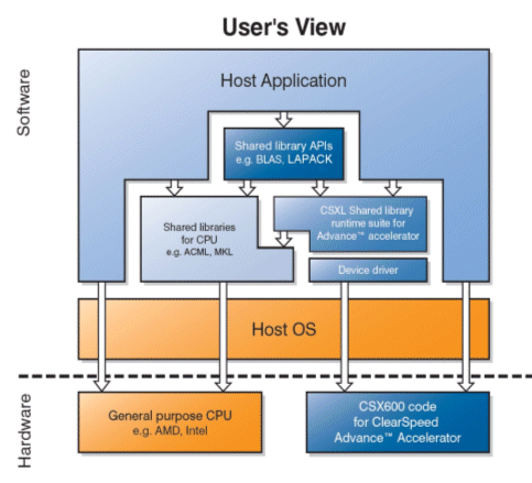
Figure 1: Overview of the ClearSpeed products
Figure 2 shows the architecture of ClearSpeed’s latest chip, the CSX700.
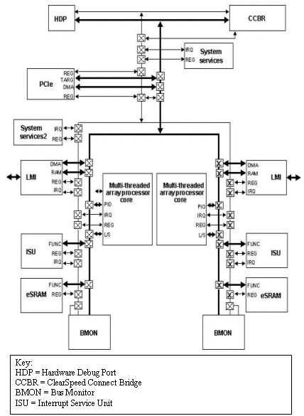
Figure 2: ClearSpeed’s current CXS700 architecture
The main changes from the previous CXS600 chip are as follows:
- Two processor cores (“MTAPs”) on one chip.
- A standard PCIe interface on the chip (vs. a proprietary PCIx-based interface).
- Several improvements to the MTAP.
Verification strategy
Overall verification needs and strategy
Figure 1 above shows the architecture of the ClearSpeed product. Ensuring the quality of this complex product leads to the following features that required verification.
- Close integration of driver code with the chips.
- Integration with a number of software libraries and applications.
- Compatibility with a range of host (OS and chipset) environments.
- High performance and low power.
Regarding the chip itself the primary verification challenge was the newly introduced PCIe interface.
In order to accomplish these verification challenges, ClearSpeed employs a state-of-the-art verification strategy appropriate to the complex design under test. There are some major themes that can be readily identified in the ClearSpeed overall verification strategy:
- ClearSpeed have been Specman users for a number of years and so the verification strategy is simulation-based with a coverage-driven pseudo-random approach.
- A hierarchical simulation strategy is used, starting at blocks and moving outwards.
- Co-simulation with software is important to help demonstrate the correctness of our product (where we regard the combination of hardware and software as our product) and also gives us a good head-start on Silicon bring-up when the chip returns. This can have a huge effect on our time-to-market.
- The software co-simulation is also performed hierarchically, starting with drivers and moving out to applications.
- Verification re-use between blocks and hierarchy.
- The use of verification IP. This has the advantage of leveraging existing knowledge from domain experts and can potentially 1 accelerate the development of the test bench.
The overall guiding verification principle is to derive the signoff criteria from ClearSpeed’s business and technical objectives at the start of the chip development. Those signoff criteria are objective and can be measured using the appropriate metrics. This provides a number of advantages including the following.
- The ability for all interested parties to agree in advance the objectives for verification.
- The ability to track progress towards verification signoff during the project.
- The ability to measure the confidence at the tapeout.
In keeping with this, the CSX700 verification signoff criteria were defined in advance. The key metrics selected were as follows.
- Functional coverage targets:
- Achieve coverage of 100% in the priority 1 coverage targets.
- Achieve at least 95% coverage in all other coverage targets and review all un-hit coverage targets.
- All system level tests written and running.
- The prototype PCIe working in all available PCIe servers.
- Review the bug discovery rate to ensure that (in conjunction with functional coverage) we were approaching a point where we believed all the most important bugs had been discovered.
- Review any outstanding known unfixed issues and assess their impact.
The PCIe verification strategy
We now discuss the PCIe verification strategy within the context of the overall verification strategy outlined above.
Block level verification
Figure 3 shows the PCIe block level test bench. ClearSpeed already had experience with AVCI and PVCI and the proprietary protocol shown in the figure, therefore the PCIe interface provided the main verification challenge. This challenge was increased by the fact that ClearSpeed were using IP from different vendors for the pipe PHY and the end point core.
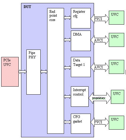
Figure 3: The PCIe block level test bench
Figure 3 shows that the test bench deploys a number of UVC’s. All but the PCIe UVC have been developed within ClearSpeed. We used our own UVC’s for other parts of the test bench – giving a homogenous eRM compliant system (subsequently uRM and now OVM).
We chose to use a third-party VIP for the following reasons.
- The complexity of PCIe protocol.
- The size of task of the verification tasks and the lack of internal resource.
- The maturity of the VIP.
- The independence of VIP being developed by an external group of PCIe experts separate to the internal development team.
We chose to use the Cadence UVC for the following reasons.
- ClearSpeed has good knowledge of e built up over a number of years. This gave ClearSpeed the confidence that it could combine the Cadence UVC with the existing ClearSpeed UVC’s to create a much more capable PCIe testbench.
- The UVC could generate controlled PCIe traffic on a per-layer basis and inject errors at each layer. This was required as ClearSpeed believed such capabilities were required to fully verify the PCIe interface.
- The Cadence UVC was highly configurable, giving us the flexibility we required to fully verify our PCIe interface.
- We had an existing relationship with Cadence that gave us the confidence that Cadence would be able to deliver a UVC of suitable quality with the features described above.
ClearSpeed also chose to use CMS in combination with the UVC for the following reasons.
- The CMS provided an existing test suite which enabled us to generate a high level of coverage out-of-the-box. It also subsequently gave us an easier and faster way to generate subsequent stimulus to hit the other coverage targets.
- The CMS practically eliminated the need to write many dozens of tests to cover various functional aspects of PCI Express protocol
- An in-built mapping of native UVC coverage points back to the PCIe specification
- Report generation and progress monitoring on a layer basis
- The ease of running the test suite and collation of test results into a coverage report.
- The ability to monitor the automated suites as they run (Is the fail rate too high? Do we need to kill it off early?)
System level
The system level test bench includes both the chip and the software driver stack. The actual software drivers are used in full except that a small change is made at the bottom of the stack where calls are made into the simulation environment and the software drives the PCIe UVC. See Figure 4 for more details. In this case the driver is doing all the things it does when talking to hardware and every transaction is passed to the simulator. This runs more slowly but does allow us to test the DMA engine etc.
The driver can connect to a simulator above the PCIe layer. This allows higher level units to be simulated without spending time fully simulating every PCI transaction. This is useful for simulating programs running on the processor.
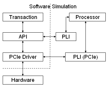
Figure 4: Software interface to the RTL simulation via the device drivers
A directed testing approach is mainly applied at the system level although by using the UVC it is possible to use constrained random stimulus where the test specification allows (e.g. in some of the data being written, in the addresses within a defined range). A number of existing directed tests existed at the system level and the main goal was to extend these to test the changes for this chip (as listed earlier). A number of vPlanning sessions were held to derive a test specification and we were then able to track implementation of those tests.
Once the driver stack is verified to be working with the RTL, it becomes possible to run higher levels of software. A number of target applications were simulated prior to tape-out (although they had to be cut down for simulation purposes):
- Mandelbrot
- DGEMM
- Biological and scientific applications such as Amber (a molecular dynamics package)
- Financial applications (such as MonteCarlo).
Running such applications gives very high confidence for functional verification but also allows performance verification too
PCIe prototyping in FPGA
During development of the CSX700 ClearSpeed produced a product based on the existing silicon (the CSX600) but with a PCIe interface in an FPGA. This allowed us to emulate the PCIe interface and perform compatibility testing. That is, we were able to connect the emulated PCIe interface to a number of servers running a variety of OS’es to identify compatibility issues in advance of tape-out. It also allows us to more thoroughly test the software driver stack interface with the PCIe.
This approach identified bugs but mainly in the physical layer of the PCIe stack (the PHY in the FPGA was different to the PHY that would be in our chip). It also put us on notice regarding the amount of variation in the PCIe implementation in the servers we were connecting to. That caused us to raise the importance of achieving very high coverage: we prioritised the coverage and set a target of 100% for the highest priority goals. However, the approach did not identify any bugs outside of the phy that wouldn’t have been found via simulation & coverage. This gave us confidence that high coverage in our PCIe simulations would give high probability of first time silicon success.
The other advantage of the prototype was in software development. It enabled the PCIe software drivers to be developed well in advance of the CSX700 silicon. This accelerated the bring-up of the CSX700 silicon once it arrived and thus sped our time to market with the CSX700-based products.
Technical details on Cadence UVC and CMS
Universal Verification Component (UVC) for PCI Express
Cadence UVCs are advanced testbench Verification IP (VIP) that provide a powerful simulated verification environment for block, chip, and system-level verification. UVCs provide the choice of using SystemVerilog and/or e based testbenches. They provide automatic stimulus generation, assertion checking, and functional coverage analysis all within a configurable, extensible, highly reusable product. In addition, the PCI Express UVC includes a highly automated compliance solution named the Compliance Management System (CMS). Each UVC includes CMS. This enables customers to greatly simplify and automate their verification. CMS delivers 70+% coverage without the need to write tests.

UVCs offer flexibility and control over stimulus generation ranging from fully random to fully directed testing. The UVC includes a powerful sequence generator that automatically creates all types of PCI Express transactions including error packets and responses. It provides both data and assertion checking, and it performs functional coverage analysis using a fully integrated coverage model.
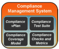
Key to the PCI Express UVC’s ability to automate compliance verification is the unique Compliance Management System known as CMS. CMS consists of a Compliance Verification Plan (vPlan), Compliance Test Suite, compliance metrics, and a compliance coverage model. The user only interacts with the vPlan and the test suite while CMS manages all the data “under the hood”. This enables the user to achieve compliance more productively and more predictably. CMS also saves time and reduces the degree of protocol expertise required.
The UVC empowers verification teams to focus on finding and fixing bugs in the proprietary functionality, corner-case, and error scenarios of the design under test (DUT). This reduces the time to bring up the verification environment, enabling the user to begin simulating earlier and thus find bugs earlier. This enables a higher quality product while incurring significantly less risk of schedule slips or product recalls. Additionally, since UVCs are all built based on the Incisive Plan to Closure Methodology (IPCM) they can be reused throughout the verification process without expending any extra effort enabling the user to retain their investment when moving from module- to block- to system-level verification or when verifying derivative products.
Benefits
- Maximizes quality with complete, easy to use protocol compliance verification
- Maximizes productivity by automating management of compliance verification to closure
- Ensures clear status communications within engineering team
- Most efficiently achieves compliance verification closure with unique automated PCI Express Compliance Management System (CMS)
- Delivers greatest predictability and team communications using metrics based compliance measurement and reporting
- Reduces protocol knowledge barrier for verification engineers new to PCI Express
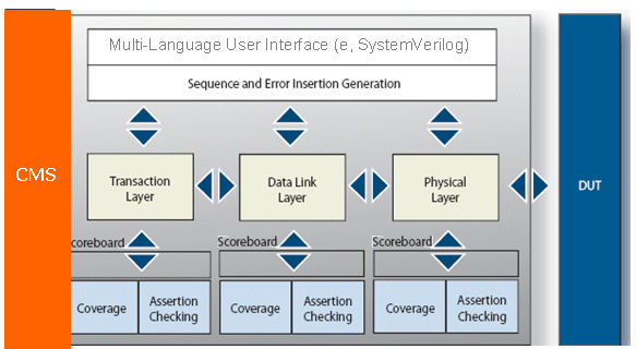
Figure 5: UVC for PCI Express block diagram
Features
Highly configurable verification environment
The Incisive UVC for PCI Express allows the user to focus on any part of the design, or on the whole design, to optimize the verification environment for the specific needs at each stage of the verification process. It is typically used to functionally verify PCI Express devices at the module, chip, and system levels. It can also be configured to selectively enable or disable each functional block, as well as the functional coverage and checking mechanisms to optimize verification on the specific task at hand. This provides the most predictable path to verification closure and maximizes your return on your investment in simulators and workstations.
Automatic stimulus generation
Unlike alternative solutions that use thousands of directed tests, the UVC for PCI Express employs an automatic stimulus generator to reduce the work the user needs to do. With automated scenario generation, including the supplied sequence library, the user can cover the major protocol functionality as well as hard-to-reach scenarios and corner cases. With the addition of a few tests, the remaining corner cases are then exercised. This approach helps the user to uncover more bugs faster and frees engineering time to focus on testing the DUT’s proprietary functionality. CMS automates this entire process.
Coverage-driven verification using CMS
CMS provides the user with an executable verification plan (vPlan). The vPlan, used together with Enterprise Manager and the built-in functional coverage model, provides the metrics needed to clearly report on what has and has not been covered. This provides the user with the roadmap and closure metrics for the verification process, giving the user a predictable verification process and clear status reporting to project or management. This methodology, known as coverage-driven verification, enables the verification team to easily identify coverage holes and focus resources on the problematic portions of the DUT.
Architected for reuse
Cadence reuse methodology enables fast bring-up of functional verification environments and ensures that UVC-based environments can be reused immediately when moving from block- to chip- to system-level verification, as well as to derivative designs. This saves time and resources by eliminating duplication of effort.
Verification of the PCIe interface (ClearSpeed)
In this section we give further details of the PCIe verification and how the UVC and CMS helped ClearSpeed to implement an improved verification strategy and added important metrics used for the tape-out decision.
Prioritisation of coverage points
By using “perspectives 2” Clearspeed was able to only consider the coverage points relevant to our implementation. ClearSpeed used the following perspective.
"Endpoint, AER = On, VC 1-7 = Off, Completer Abort = Off, Config Request Retry Status = Off, Poisoning = Off"
The CMS allows reporting coverage by the major PCIe blocks: TPL, TXN, DLL, PHY, PMG, SYS and CONFIG. This helped ClearSpeed to prioritise our verification effort based on technical risk.
- We considered that the physical layer was a higher risk because we had two different IP vendors straddling the PHY layer and the PHY layer not covered in FPGA proto testing (as the FPGA used a different PHY)
- Power mgt was next highest priority because it was not covered in the FPGA prototype (for technology restriction reasons)
- The data link layer was the next level priority because it was next to the PHY.
ClearSpeed also required a finer grain of prioritisation: prioritisation within the blocks. Although in general prioritisation can be achieved using perspectives, this approach may not be able to address all the needs and use models of prioritisation. It is missing the finer granularity and some of the re-use aspects which are more important for expert users of CMS (such as Clearspeed and IP developers). Cadence is moving forward with improving prioritization in each new release.
Compliance test suite
The CMS provides compliance tests which give a very good base coverage to start with and so a quick start on the verification. ClearSpeed were an early-access and were receiving updates (additional coverage items and compliance tests) throughout the project so the % coverage achieved with the compliance tests varied during the project. Cadence now estimates that a customer should be able to achieve approximately 70% coverage just through the use of the CMS test suite out of the box.
The CMS tests can also be configured to get into corner cases within the PCIe protocol. ClearSpeed then wrote a number of our own tests to drive the UVC to get the coverage to the expected level.
Tracking confidence using coverage data
ClearSpeed tracked progress through the coverage data. As mentioned before, this was broken down into the major PCIe blocks so that we could adapt resource by assigning people to write tests targeted at specific blocks.
Figure 6 provides example PCIe coverage data trends broken down into the major PCIe blocks. Please note that this does NOT represent the actual coverage achieved by ClearSpeed as this is confidential and the dates have also been removed. However, it does represent the sort of graph that ClearSpeed achieved and were able to use to track confidence as we progressed towards tapeout. Note that the coverage starts below the approximate 70% coverage achieved just through the use of the CMS test suite out of the box because (as already noted) ClearSpeed were an early adopter and were using the UVC before all of the test suite had been implemented.
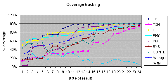
Figure 6: Example structured PCIe coverage data broken down by category
Tracking of coverage data using the above graph was the main management tool in reporting progress towards out tape-out signoff criteria and assigning resources accordingly.
Use of structured coverage data at signoff
At about 4 weeks before tapeout ClearSpeed began the review of the coverage holes. In all there was about 80 items to review (from an initial coverage space of over 200,000 buckets although some of the 80 items had multiple buckets). For each we were able to assign a risk based impact and probability (derived from an assessment that the lack of coverage might mean that we had a missed a bug). Appropriate actions could then be assigned. The fact that the missing coverage was structured into the various PCIe blocks allowed ClearSpeed to prioritise the review and the subsequent actions.
By signoff ClearSpeed had reduced the coverage holes significantly from 80 and was able to review each remaining hole in detail and waive based on a risk assessment.
Bug tracking
CMS allows the user to track fail rates and causes. We used this to augment our internal bug tracking tool to perform bug tracking specific to the PCIe.
Use of external resource
As ClearSpeed were using commercially supplied VIP meant that there was external resource available with experience in using the UVC and CMS allowing us to rapidly bring in external resource to top up our coverage. The external resource was used to improve our transaction level coverage and the externally developed tests mapped quickly into our test suite environment.
Lessons learned
ClearSpeed learned a variety of lessons when using metrics-driven verification:
- The use of CMS does allow the user to quick-start their verification and to subsequently fill coverage holes as the project progresses.
- The splitting of the coverage goals into the functional areas allows for easier prioritisation, resource allocation and project tracking.
- The CMS tools need to better support the prioritisation of coverage points.
ClearSpeed also provided inputs to Cadence about usage models and capabilities desired for its UVC and CMS. These include:
- Better filtering features in the Compliance vPlan are needed
- Prioritisation of coverage sections and items are needed
- CMS value would be even further enhanced with additional pre-defined tests to cover even more corner case scenarios.
Conclusions
The verification approach ClearSpeed adopted has proven to be highly successful, This approach, based on metrics-driven verification and employing third party VIP, exceeded our expectations and successfully verified the integration of existing IP into the ClearSpeed chip. As evidence of this success ClearSpeed has achieved first time silicon success on the CSX700 chip as demonstrated by:
- Successful compliance testing results including the first time success in all machines at the PCIe PlugFest in February 2008
- 100% successful boot cycle testing results over a number of servers and chipsets.
- Successful integration with ClearSpeed’s full suite of supported OS’es 3 over all available servers.
- All performance and power targets were met.
References
1. “Verification - it's all about confidence”, Mike Bartley. SNUG 2001, Munich.
Notes
1. Since writing this article, one on the authors, Mike Bartley, has left the employment of ClearSpeed and now is providing independent verification consulting services (mike at tandvsolns dot co dot uk). ClearSpeed remains committed to the verification approach described in this article.
1 We use the term “potentially” through experience. Badly developed VIP can be harder to integrate and use than developing it yourself. Fortunately industry-wide methodologies such as OVM are improving the VIP experience.
2 Perspectives are used to mask out coverage sections/items irrelevant to your DUT
3 We use the term “potentially” through experience. Badly developed VIP can be harder to integrate and use than developing it yourself. Fortunately industry-wide methodologies such as OVM are improving the VIP experience.
Related Semiconductor IP
- Configurable PCI Express 4.0 Link Controller
- PCI Express PHY
- Multi-Channel Flex DMA IP Core for PCI Express
- PCIe - PCI Express Controller
- PCI Express PIPE PHY Transceiver
Related Articles
- Achieving Compliance and Interoperability for Your PCI Express Design
- Learning not to fear PCI Express compliance
- How HyperTransport and PCI Express complement each other
- Advanced switching boosts PCI Express
Latest Articles
- An FPGA-Based SoC Architecture with a RISC-V Controller for Energy-Efficient Temporal-Coding Spiking Neural Networks
- Enabling RISC-V Vector Code Generation in MLIR through Custom xDSL Lowerings
- A Scalable Open-Source QEC System with Sub-Microsecond Decoding-Feedback Latency
- SNAP-V: A RISC-V SoC with Configurable Neuromorphic Acceleration for Small-Scale Spiking Neural Networks
- An FPGA Implementation of Displacement Vector Search for Intra Pattern Copy in JPEG XS