Optimizing Floorplan for STA and Timing improvement in VLSI Design Flow
By Sunandan Choubey, Sandeep Mall (eInfochips, An Arrow company)
Abstract
Static timing analysis is a technique of computing of cell delay and interconnect delay in design (known as path delay) and comparing it against constrain (timing specific) set in SDC file. This paper describes the static timing analysis for a specific design mainly about mem2reg reg2mem and reg2reg setup analysis a kind of detecting and solving the setup violation in design.
I- INTRODUCTION
This is a full chip design, which consists of around 23 macros, and operational frequency is 55Mhz. It consists of memory, regulator (analog block), analog-to- digital converter, as shown in the fig 1.0, and several other macros. This is the initial floorplan and location of all the i/o pads, which is used during PNR stage. With this floorplan we have seen major timing violation in mem2reg path in system mode after completion of routing stage.
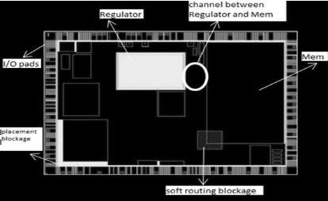
Fig 1.0 Represent design and its component
For any chip, before moving to fabrication stage, static timing analysis is mandatory, so that we can reduce timing violations. The initial level of checking/diagnosis for the chip is timing check and in timing checks we do setup time, hold time, recovery, removal, etc. In this paper, we will discuss setup check and the technique used for resolving it.
Timing checks requires following terms:
- Timing path: Timing paths in a design can be considered as a collection of paths. Each path has a startpoint and an endpoint. In STA, the paths are timed based on valid startpoints and valid endpoints. Valid startpoints are input ports and clock pins of synchronous devices, such as flip-flops and memories. Valid endpoints are output ports and data input pins of synchronous devices. Thus, the valid timing paths in Fig 1.2 be:
- input port A to UFFA/D,
- input port A to output port Z,
- UFFA/CLK to UFFB/D, and
- UFFB/CLK to output port Z.
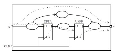
Fig 1.2 Various timing path
- Data path: A path between UFFA-Q and UFFB-D which goes through a various combination logic cell.
- RAT: Required arrival time is expected time for signal to arrive end point from start point. It defines the design needs like operating frequency.
- AAT: Actual arrival time is time required reaching end point from start point and it is always calculated at end points.
- Slack: Difference between arrival and required time. Min slack/hold slack/min difference=AT-RT Max Slack or Setup slack or max difference=RT-AT.
- Reg2reg analysis: Timing path from launch flip-flop clock port to capture flip-flop d pin which includes two registers (flip-flops), so reg2reg. Here the UFFA is considered as lunch flop and UFFB is a capture flop. Similarly, for mem2reg path in mem2reg data will lunch from a memory block and capture by a flop or register.
- WNS, TNS and FEP: WNS is worst negative slack of timing path where TNS is the total negative slack, which is the sum of all WNS in design. FEP describes the total failing endpoint of design.
- Setup check: A setup check ensures that the data can arrive at a capture flip-flop within the given clock period. It can be understood by a simple example, shown in Figure 1.3(i) and 1.3(ii), where both the launch and capture flip-flops have the same clock.
- The first rising edge of clock CLKM appears at time Tlaunch at launch flip-flop. The data launched by this clock edge appears at time Tlaunch + Tck2q + Tdp at the D pin of the flip-flop UFF1.
- The second rising edge of the clock (setup is normally checked after one cycle) appears at time Tcycle + Tcapture at the clock pin of the capture flip-flop UFF1.
- The difference between these two times must be larger than the setup time of the flip-flop, so that the data can be reliably captured in the flip-flop.
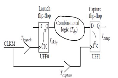
Fig 1.3(i) Timing analysis
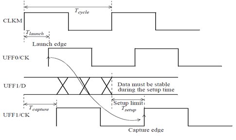
Fig 1.3(ii) Clock representation of setup check
The setup check can be mathematically expressed as:
Tlaunch + Tck2q + Tdp < Tcapture + Tcycle – Tsetup
II- COMPLICATION WITH DESIGN
There is setup violation for the worst condition of setup check after completing the route_opt stage. In mem2reg total 637 violating path with worst negative slack is -1.204(ns), in reg2mem only one path violating with -0.227(ps) and in reg2reg there are 42 violating path with worst negative slack is -0.358(ps) as shown in Fig 1.4 and this is the timing report for the floorplan fig 1.0
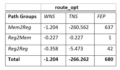
Fig 1.4 Table of timing violation at post route.
III- ANALYSIS OF DESIGN
The worst path of design in mem2reg path is as shown in Fig 1.5, where the start point of memory and the end point of register are not distant from each other, but the data path is substantially large. Due to this, the delay of data path is high enough to cause setup violation in design.
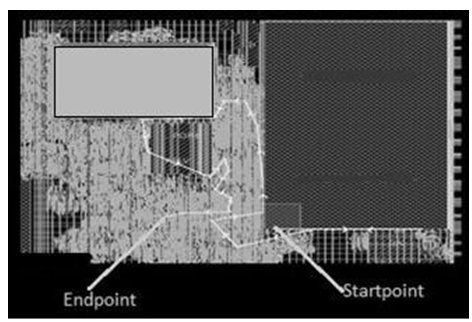
Fig 1.5: Representation of a mem2reg path
To identify the complication with the data path, on why the data path is substantially huge, we have plotted hierarchical standard cell placement of the design is as shown in Fig 1.6. Here we can observe that all the hierarchical standard cell related to memory is placed between the channel formed by regulator and memory. And all the other endpoint register is placed downward near the macro related to those register. Due to this, the data path of the design has to pass through a long path between start point and the endpoint.
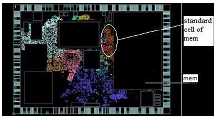
Fig 1.6: Standard cell placement in design
Therefore, if we observe the entire violating data path between mem2reg and reg2mem we can identify similar pattern as shown in fig 1.7(i) and fig 1.7(ii) respectively.
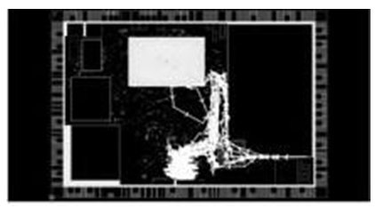
fig 1.7(i) All mem2reg violating path
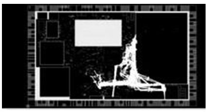
fig 1.7(ii) All reg2mem violating path
IV - RESOLVING TECHNIQUE USED
We have seen that the data path in both cases are too large. The start point and end point are near to each other but due to the bad placement of standard cells the data path of mem2reg is getting too large. Therefore in the new floorplan the channel between memory and regulator is covered with soft placement blockage fig 1.8 and the regulator is shifted upward so that tool optimizes the placement of standard cell placement and try not to place any standard cell between the channel so that the data path between mem2reg and reg2mem can be reduce. After the change in floorplan, the new result is shown in fig 1.9 so it is an iterative process.
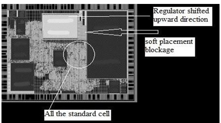
Fig 1.8 Placement of standard cell with modified floorplan
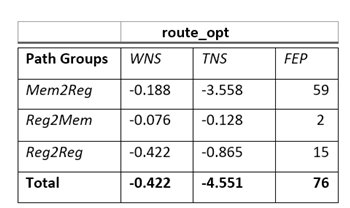
Fig 1.9 Post route timing data after experiment
CONCLUSION
With this iterative experiment timing has been significantly reduced from WNS -1.204(ps) with total 637 path to WNS -0.188(ps) with total 59 path for mem2reg path. Moreover, for reg2mem path total violating paths has been reduced from to 42 to 15 paths.
REFERENCE
- Chuck Monahan, Forrest Brewer, Concurrent Analysis Techniques for Data Path Timing Optimization.
- J Bhasker, Rakesh Chadha, Static Timing Analysis for Nanometer Designs A Practical Approach.
- M. Mahmood ; M. Chandrasekhar ; B. Sharma, A method of timing driven data path synthesis.
- G. Siva Priya; K. Hari Kishore; Fazal Noorbasha, Static Timing Analysis and Timing Violations of Sequential Circuits.
Authors
 | Sunandan Choubey Physical design engineer working with eInfochips, An Arrow company. He has more than 2 years of experience in ASIC design, includes various technology nodes like 16nm, 28nm. |
 | Sandeep Mall Physical design engineer working with eInfochips, An Arrow company. He has more than 2 years of experience in ASIC design, includes various technology nodes like 22nm and 16nm. |
Related Semiconductor IP
- NPU IP Core for Mobile
- NPU IP Core for Edge
- Specialized Video Processing NPU IP
- HYPERBUS™ Memory Controller
- AV1 Video Encoder IP
Related White Papers
- Differentiation Through the Chip Design and Verification Flow
- AI, and the Real Capacity Crisis in Chip Design
- Emerging Trends and Challenges in Embedded System Design
- Integrating VESA DSC and MIPI DSI in a System-on-Chip (SoC): Addressing Design Challenges and Leveraging Arasan IP Portfolio
Latest White Papers
- Transition Fixes in 3nm Multi-Voltage SoC Design
- CXL Topology-Aware and Expander-Driven Prefetching: Unlocking SSD Performance
- Breaking the Memory Bandwidth Boundary. GDDR7 IP Design Challenges & Solutions
- Automating NoC Design to Tackle Rising SoC Complexity
- Memory Prefetching Evaluation of Scientific Applications on a Modern HPC Arm-Based Processor