Optimized Clocking Solutions for High-Performance Die-to-Die Interfaces
By Blake Gray, Jeff Galloway, Randy Caplan — Silicon Creations
Introduction
The economics of a system-on-chip ASIC have evolved over the last decade, driven by forces such as cost to yield a transistor, wafer defect density and chip yield, and the drive for greater performance and efficiency. As process nodes continued to shrink from 28nm down to 3nm, we observed Moore’s Law begin to break down, and the cost to yield 100 million transistors normalized to 28nm was either flat or, arguably, increased. Figure 1 is a graph presented by Milind Shah at the 69th IEEE International Electron Devices Meeting demonstrating this phenomenon.
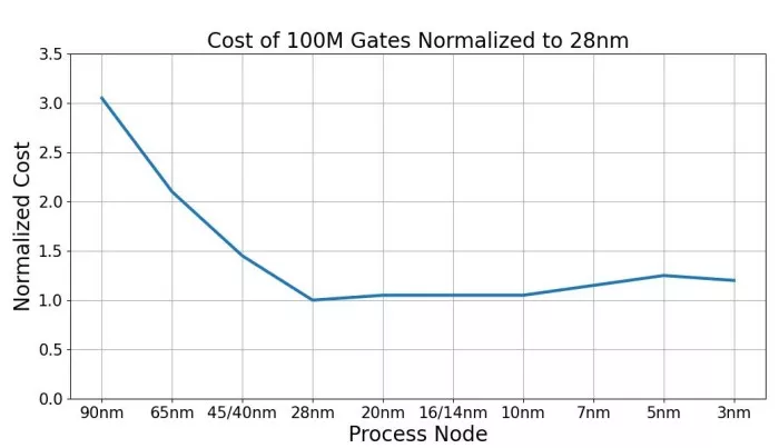
Figure 1- Cost to yield 100M transistors vs. process node, normalized to that at 28nm.
Despite the stalling of cost scaling, we continue to see the industry advancing toward ever-smaller transistors. Leading-edge technology associated design costs are increasing as well. It begs the question: why the industry push? Simply put, at the systems level, the drive for smaller nodes enables tighter integration of components on the chip, leading to improved performance and enhanced power efficiency. However, this lack of cost scalability makes adopting the latest nodes less attractive for some chip designs.
Advanced process nodes, such as TSMC’s N10, N7, and N6, boast defect densities at or below 0.1 defects per square centimeter. While impressive, CPU and GPU dimensions continue to grow, driving down chip yields as die sizes approach the reticle limit, as seen in Figure 2.
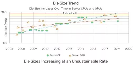
Figure 2 - CPU/GPU die size vs time. Source: AMD
These factors (and certainly others not discussed here) encourage disaggregating designs into chiplets rather than creating monolithic chips from a single piece of silicon. Certainly, chiplets may not make sense for designs that either cannot be efficiently disaggregated or are challenging to disaggregate due to manufacturing complexities.
Die-to-Die Interfaces - UCIe
Within the evolving ecosystem of chiplets, there are many design challenges that must be addressed. Die-to-die (D2D) interfaces are especially noteworthy in industry, particularly the performance requirements of the clocking solution. There are several available D2D interconnect protocols, such as Open High Bandwidth Interconnect (OpenHBI), Bunch of Wires (BoW, part of the Open Compute Project), Extra Short Reach (XSR), Chiplet Interconnect Express (CIE), and Intel’s Advanced Interface Bus (AIB). In this article, we will focus on Universal Chip Interconnect express (UCIe).
UCIe is an open, multi-protocol, layered, on-package D2D interconnect standard that supports a range of data rates from 4GT/s up to 32GT/s. It enables a flexible ecosystem for disaggregated die architectures by supporting protocols like PCIe, CXL, and customizable raw modes over a shared physical and link layer. While 3D packaging is currently not supported, standard low cost (2D) and advanced high performance (2.5D) packaging options are, either chosen based on application needs.
The main data path sits in the Physical Layer, where the clocking solution, FIFO, and SERDES reside. In Figure 3 we call out the transmitter/clocking architecture within the SERDES, highlighting in green the clocking solution.

Figure 3 - Advanced (2.5D) package with callout for the transmitter/clocking architecture in the Physical Layer. The clocking solution is highlighted by a green box.
There are multiple design challenges associated with the clocking solution. Here we identify and discuss 4 critical performance metrics that must be considered when choosing one for a D2D interface:
- Low power
- Ultra-low period and N-cycle jitter
- Small form factor
- Wide tuning range
Critical Performance Metrics - Low Power
The UCIe protocol defines key performance targets, one of which is energy efficiency, as summarized in Table 1 for several supported data rates, package styles, and channel reach.
Table 1 - UCIe key performance targets for energy efficiency. N = interface width.

Note that the energy efficiency numbers seen in the above table includes all Physical Layer circuitry: Tx, Rx, PLL, clock distribution, etc., and are normalized to the interface width, N. These aggressive efficiency targets mandate low power consumption of the Tx clock generation circuit to maintain ample design margins for the remaining Physical Layer components.
Critical Performance Metrics – Ultra-Low Period and N-Cycle Jitter
Figure 4 shows the full clocking architecture in a die-to-die communication example, complete with annotations highlighting the clocking solution (in green) and the forwarded clock (in purple).
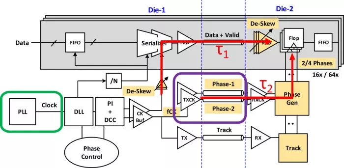
Figure 4 - Clocking architecture. Highlighted in green is the clocking solution, and in purple the forwarded clock.
A feed-forward clocking architecture naturally filters low-frequency jitter, assuming the propagation delay difference between the data and the clock is small, i.e. |τ_1-τ_2 | is minimal, where Τ1 and Τ2 are the phase propagation delays for the data path and clock path, respectively. In this case, the timing jitter is correlated and common between the data and clock.
Now, consider an example where the phase propagation delay between the data and forwarded clock path is unequal, exceeding several UI, as seen in Figure 5.

Figure 5 - Unequal Data/CLK phase delay example. Τ1 > Τ2.
In this example, unequal Data/CLK delay from the Tx to the Rx (Τ1 > Τ2) causes the sampling edge to arrive early, resulting in the wrong CLK edge to clock the data at the Rx flop. As the Data/CLK propagation time delta grows, high-frequency uncorrelated jitter has an opportunity to accumulate in the data phase, potentially resulting in bit errors and degrading the BER. Period and N-cycle jitter (for small N) are of particular concern. Thus, eliminating or minimizing sources of high-frequency jitter within the clocking architecture is critical to maintaining target BER at the Rx.
Critical Performance Metrics – Small Form Factor
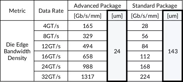
In a D2D interface, the area closest to die edge is prime real estate, typically reserved for the circuitry that passes the data and clock from Tx to Rx. UCIe defines limits for die edge bandwidth density that, when decoupled from data rate, simply limits the area the selected configuration can consume, as seen in Table 2. It’s unlikely that the clocking solution would sit on the die edge. Nevertheless, small form factor is important to allow for optimal placement and integration into the TX without jeopardizing SERDES performance.
Table 2 - Die edge bandwidth density vs. supported data rate.
Critical Performance Metrics – Wide Tuning Range
Given the aggressive energy efficiency per bit requirements seen above in Table 1, a half-rate SERDES architecture is likely necessary. Table 3 provides the required clock frequencies at each UCIe supported data rate.
Table 3 - Clocking solution clock frequency vs. supported data rate for half-rate SERDES architecture.
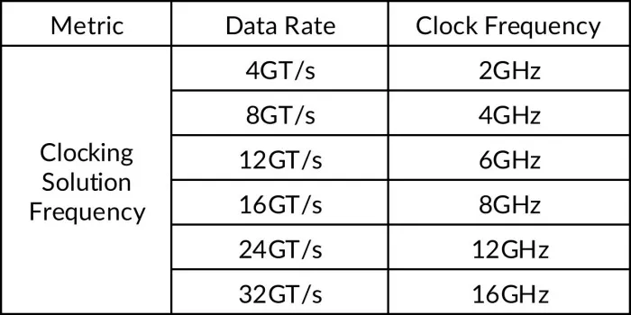
There are clear advantages: (1) a half-rate architecture reduces the maximum operational clocking solution frequency by half, (2) a single, wide tuning range clocking solution can support all UCIe data rates, and (3) postdivision provides the system designer a means to optimize the tradeoff between power consumption and jitter.
Optimized Clocking Solutions
Given the design and performance challenges presented above, our attention now turns to available options for the clocking solution. Figure 6 outlines our objective and 3 clock synthesis circuits we believe are appropriate choices.
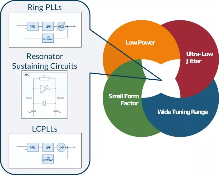
Figure 6 - Clocking solution options to meet the performance demands of D2D interfaces.
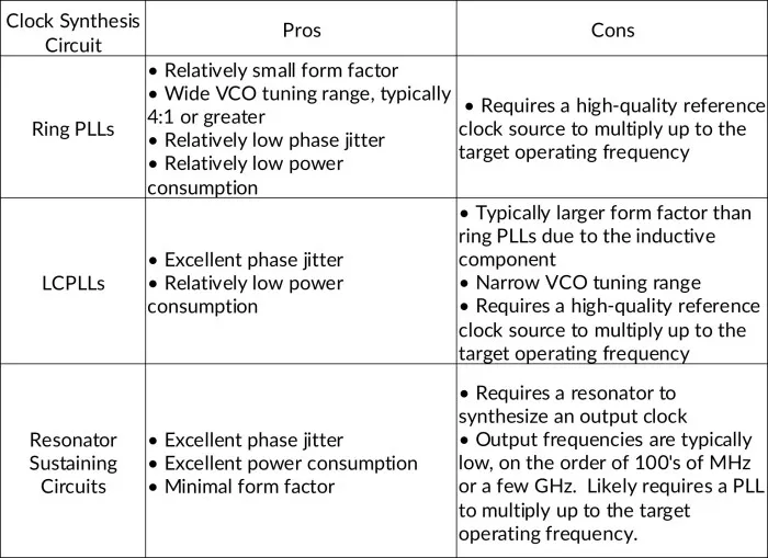
Table 4 summarizes the pros and cons of each clock synthesis circuit.
Table 4 - Clock synthesis circuit pros and cons as options to be the clocking solution in a D2D interface.
Silicon Creations D2D Clocking Solution
Silicon Creations is well positioned to provide quality clocking solutions for D2D interfaces in a wide range of foundries and process nodes. For example, consider the clocking solution seen in Figure 7.
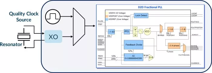
Figure 7 - Silicon Creations D2D Optimized Fractional-N ring PLL.
This dedicated D2D ring-based fractional-N PLL was developed for TSMC 3nm FF but is easily portable to other process nodes. The PLL can be driven by any quality clock source, or even a resonator-based oscillator for high-performance applications.
Let’s consider this clocking solution for an advanced package, 24GT/s long-reach D2D application, 40-bit data width:
Critical Performance Metric
- Low power
- For this application, the maximum power consumed by the Physical Layer is specified as 9.6mW x 40 = 384mW.
- Assume the PLL is operating at a PFD frequency = 100MHz, VCO frequency = 12GHz.
- The following table summarizes the power consumption of the PLL. Note that N3 is a 1.2V IO, 0.75V core process.
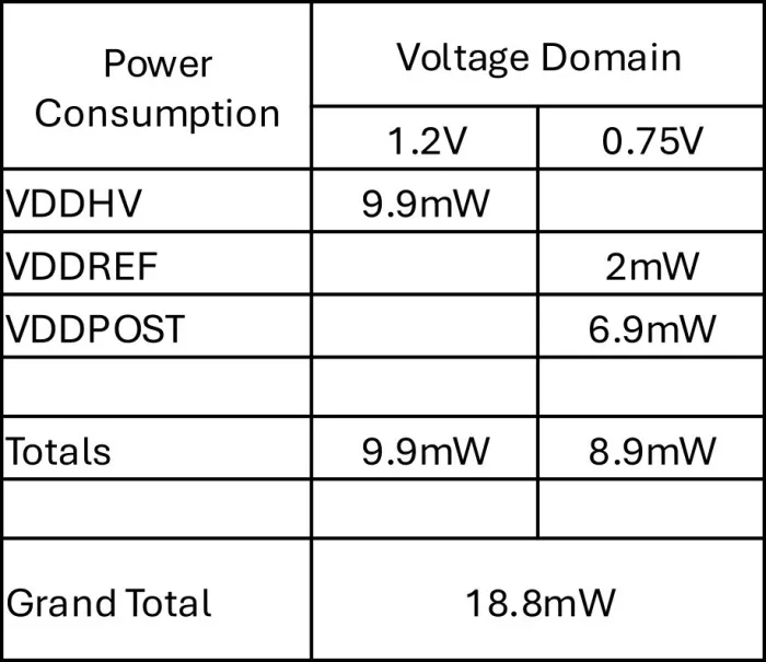
- At 18.8mW, the PLL accounts for only 18.8mW / 384mW = 4.9% of the power budget for the Physical Layer.
- Ultra-low jitter
- The specified maximum period jitter over PVT for this PLL is 160fs RMS at FVCO = FOUT = 12GHz.
- Small form factor
- Die size for this process is 110μm x 110μm, or 0.012mm2
- This is likely too large to be placed at die edge given target bandwidth density. However, the PLL can clock multiple lanes and spread out its area impact.
- Die size for this process is 110μm x 110μm, or 0.012mm2
- Wide tuning range
- Input frequency range – 80MHz to 2.5GHz
- Output frequency range – 100MHz to 12.8GHz
Conclusion
Chiplets have enabled a powerful new ecosystem of system-on-package, driven in part by the economics of advanced semiconductor processes and technologies. The D2D interface is a critical subcomponent of any chiplet design and the clocking solution can make-or-break it. Immense performance requirements of the clocking solution (ultra-low jitter, low power, wide tuning range, and small form factor) mandate careful design considerations and optimization tradeoffs. The Silicon Creations clocking/XO sustaining circuit IP portfolio is well positioned to meet the demands of D2D designs.
Related Semiconductor IP
- General-purpose & Specialized Ring PLLs + RTL-based Solutions
- NPU IP Core for Mobile
- NPU IP Core for Edge
- Specialized Video Processing NPU IP
- HYPERBUS™ Memory Controller
Related White Papers
- New Embedded DRAM Solutions for High-Performance SoCs
- Software Infrastructure of an embedded Video Processor Core for Multimedia Solutions
- LPDDR flash: A memory optimized for automotive systems
- Why Interlaken is a great choice for architecting chip to chip communications in AI chips
Latest White Papers
- Ramping Up Open-Source RISC-V Cores: Assessing the Energy Efficiency of Superscalar, Out-of-Order Execution
- Transition Fixes in 3nm Multi-Voltage SoC Design
- CXL Topology-Aware and Expander-Driven Prefetching: Unlocking SSD Performance
- Breaking the Memory Bandwidth Boundary. GDDR7 IP Design Challenges & Solutions
- Automating NoC Design to Tackle Rising SoC Complexity