Automated On-the-Fly Verification of Designs Using Detector-Based Methodology
By Dirk Dammers, Wei Guo, Frédéric Masson, Lars M. Voßkämper Dolphin Integration
ABSTRACT
Mixed-signal simulation of systems, i.e. analog & digital electronics with attached peripherals, such as sensors and actuators, already has an essential place in today’s design process. While the verification of the digital parts, mostly implemented in Verilog and VHDL, has gained a speed and quality increase through the use of Assertion-Based Verification (ABV) with Property Specification Language (PSL) and System Verilog Assertions (SVA), analog verification suffers from not being supported by these assertion description languages. To speed up and secure the verification of the analog parts (SPICE, Verilog-A(MS), VHDL-AMS), innovation is needed.
Based on the assertions approach, this paper presents an innovative methodology for the verification of analog and mixed-signal circuits which embeds detectors at each step of the hierarchical verification process to increase Quality Control and reduce Time to Market. This paper illustrates the approach with the input range and phase shift verification of the Analog Front-End (AFE) of an Energy Meter. It does not discuss strategies to verify the complete functionality of the design.
Index Terms— mixed-signal design verification, design debug, detectors, specification, assertion.
1. INTRODUCTION
Much like assertions for Assertion-Based Verification (ABV), this new methodology targets the verification of analog, mixed signal and multi-domain designs by providing the means to embed so-called detectors into the design and/or test bench. A dedicated library provides a set of ready-to-use detectors, as well as fundamental elements which can be assembled to graphically create custom detectors by drag and drop in a schematic editor. Detectors can be used early in the design process to observe automatically the circuit behavior, check whether specifications (functional, device properties) are met and reliably announce violations. Moreover, they offer debugging possibilities through the option to pause or abort the simulation and also thanks to the generation of messages issued in the simulation log. Analysis of the order of events is simplified thanks to the identification of the time and location of errors.
Detectors are virtual devices for on-the-fly processing during transient simulation. They are embedded into the circuit components or test bench to observe physical domain quantities, such as voltages or currents, and check whether operating conditions or connection conditions are respected, for instance by testing whether a value is above, below, within or outside a specified range on a specific event or within a defined time window. Networks of detectors can be created by interconnecting them to perform more complex checks and detections including calculations.
2. RELATED WORK
Over the years, there have been several publications focusing on verification of analog and mixed signal designs. They can be separated into on-the-fly and post-processing methodologies.
The post-processing verifications do not affect the simulation time as they are performed at the end of the simulation, but additional time is needed to perform analyses. They also allow using additional tools such as Matlab or Mathematica to perform investigations e.g. through Fourier analyses.
The on-the-fly methodologies provide results during simulation. They allow aborting faulty simulations, therefore avoiding useless simulation runtime and starting earlier the debugging process. Such methodologies can have an impact on the simulation time.
In [1], [2] an online monitoring approach based on a System of Recurrence Equations (SRE) is presented to be able to use PSL for observations. Here, for continuous time components, the time domain differential equations (DAE) have to be converted to recurrence equations, which are the discrete version of DAE’s. Since it is difficult to observe analog signals/properties in PSL, the PSL properties have to be converted into SRE notation. This solution requires using a special simulator (C-SRE) as the models are not implemented in a standardized Hardware Description Language (HDL).
In [3] a special simulator (MLDesigner) is used to support the composition of system models by using model fragments with different domain models (continuous timediscrete event for analog and mixed signal parts, discrete event for digital parts) of computation. In this approach, analog assertions are transferred into PSL, which is an industry standard for formal digital assertions.
In this paper, we combine the approach of an HDL detector library as described in [4] with the approach of a reusable, extensible building block library of fundamental elements as described in [5] to create a library that enables to build easily reusable detectors.
As result, we obtain a library, implemented in standardized HDL, that can be used in any mixed signal circuit simulator, supporting VHDL-AMS and/or Verilog-A, for verifying designs in transient simulations, which represent new solutions for mixed signal validation compared with state of the art in [6].
2. THE DETECTOR METHODOLOGY
The vision that led to the implementation of the detector library was to improve design security and quality of analog and mixed-signal designs through automated and reliable verification and avoidance of manual waveform analysis.
Detectors are built to observe specific system characteristics, e.g. to measure currents, voltages, frequencies, slopes, delays, jitters etc., on the condition to not influence the behavior of the design under simulation. So, detectors are passive "observers" with respect to the circuit. However, they are active with respect to the user: detectors announce on-the-fly, during simulation, when signals violate specification rules and log these events in report files for further analysis. Depending on the severity level set up for the alerts, the simulation can be aborted, paused or continued for debugging purposes.
Figure 1 shows the typical detector structure, which is an assembly of fundamental elements. The core of the detector library provides the internal functions as listed below:
- Probes (1) (mandatory): monitor a value, optionally a differential value (I) in the circuit and convert a physical domain flow or potential quantity to a real quantity. This quantity is the value that a checker can observe directly, or it can be an input for a calculator.
- Triggers (2) (optional): used to activate a checker.
- Calculators (3) (optional): used to calculate a value that must be observed but is not directly accessible in the circuit, e.g. for the electrical domain, the measurement of the power factor can be combined with the current and voltage measurement to give the instantaneous active and reactive power. The inputs are generally the outputs of probes or of other calculators.
- Checkers (4) (mandatory): observe if the input quantity stays within its limits or not. A checker is enabled via a boolean “true” at the ENABLE input. If the input is out of the limits, i.e. in case of a violation, the TRIGGER will be “true”. The input of a checker is generally the output of a probe or of a calculator. Checkers are generally activated by triggers or other detectors.
- Messengers (5) (mandatory): announce violations to the user, on the screen and/or in a log file, when ENABLE is “true”. Depending on the severity level, the simulation can be paused or aborted.
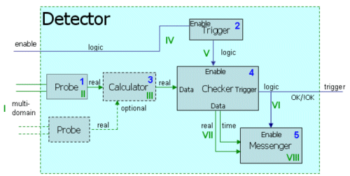
Figure 1: Typical structure of a detector
The above mentioned fundamental elements can be combined to build any thinkable detector. The general structure of a typical assembled detector consists of:
- input value(s) (I) that are observed (monitored and converted using a probe (1)),
- a trigger that enables the observation (2),
- an optional calculator that calculates the value to observe out of the input value(s) (3)
- a checker that checks if a specification violation occurs (4) and
- a messenger that reports the violation (5)
While implementing the detectors, special focus was put on being compatible with any possible application, for instance through parameterization, in order to be adaptable to different specifications.
3. DESIGN VERIFICATION PROCESS
The verification flow of this proposed methodology is shown in Figure 3. The fundamental detector elements will be interconnected, graphically as blocks in the schematic editor, depending on the specification/functionality to check. The resulting assembled detector can be used in the design to observe specification violations during simulation. If needed, the detector log files can be analyzed for further investigation during debug.
Contrarily to PSL based mixed-signal verification approaches, this methodology makes use of the standard analog Hardware Description Languages (HDL) VHDLAMS and Verilog-A(MS) to build a library of detectors. This ensures that designers using different simulators supporting multiple languages (Verilog(-A(MS)), VHDL(- AMS), SPICE...) can benefit from these developments and are not bound to special simulators or simulator couplings. This facilitates their instantiation in multi-language circuits. It also allows monitoring online design specification violations while performing simulations of any hierarchical level (architectural, behavioral, functional and electrical).
Figure 2 illustrates the application of the detectors in circuit design, transfer and System-on-Chip (SoC) Integration.
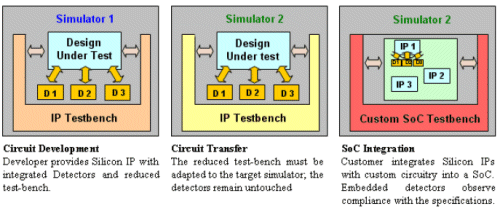
Figure 2: Detector featured Mixed-Signal Design and Circuit Transfer
For circuit design, detectors speed up the verification process through automatic specification rule checks. The detectors replace proprietary simulator specific test bench code with independent detectors embedded in the model. Thanks to the use of standard HDL, the same detectors can operate in different simulator environments without the need to adapt the test bench, which means that the model of the Silicon IP can be delivered to a customer to check whether it behaves as expected in the customers' environment. For SoC Integration, embedded detectors enable checking that integration rules are respected, verifying that specifications are met and detecting unexpected component interactions when integrated into a SoC. The main benefit is that SoC Integrators do not have to perform manual, and error prone, checking of a huge amount of signals in order to verify that specifications are met and thereby get a reliable feedback. All the specification rules that are implemented by the detectors are checked automatically during the simulation.
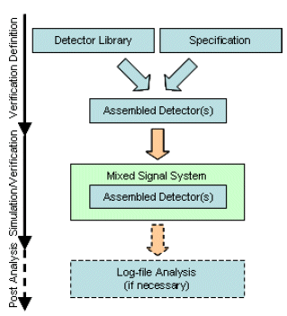
Figure 3: Verification flow
During system design, this methodology can also be used for equivalence checking of models at different abstraction levels. For complete SoCs, the simulation of the whole design with transistor-level models is not realistic because of the long simulation time and of the computing effort required. Therefore, transistor-level models of subsystems will be replaced by behavioral models. It has to be ensured that the replacement model is equivalent on its interface to the circuit. Figure 4 shows how detectors help to verify that both the transistor level and the behavioral model have the same “detector outputs” when the same test patterns are applied.
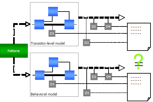
Figure 4: Detector-based equivalence checking
The advantage of using a library of detectors, rather than using a special language, is that already verified models can be reused and the libraries remain untouched.
4. ADVANTAGES OF METHODOLOGY
As the detectors can be integrated into schematics, this implies that the Design of Experiments based on these checkers is kept at each step of the bottom-up process: the integration of schematics at a higher hierarchical level is secured by the detectors which embed usage verification. Consequently, designers save time by not having to define again necessary consistency verifications as the design is instantiated with its embedded detector(s), as a selfcontrolled black-box. For analog design, if used in a schematic editor which enables selective netlisting to filter detectors for layout netlist, the same reference schematic can be used both for simulation and for layout.
Moreover, as detectors are on-the-fly checkers, when an error occurs, the designer is immediately informed and can perform debug without waiting for simulation end. Furthermore, design robustness checks with many parameter variations can be performed in batch mode and the detectors can help identify sensitive parameters by reporting simulation runs which were out of specification.
In conclusion, it implies that detectors increase the Quality Control in a lower lead-time, and accelerate the final Time-to-Market.
5. THE DEMONSTRATOR
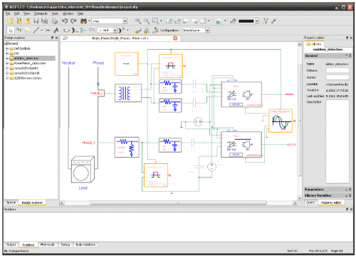
In the illustrative design example of Figure 5, the two Analog Front-Ends (AFEs) digitize the two analog input signals (sinusoidal waves of current and voltage) respectively, and then output the digitized data to the computation unit which handles the power calculation in digital manner. As this paper focuses on the verification of the analog part, Figure 5 only represents the analog part of the entire power meter design.
Figure 5 illustrates an example of the use of two kinds of detectors with their input range specifications:
D1 and D2 are indeed the same type of detectors with different parameters (0.8 Vrms maximum for differential current channel input, 0.4 Vrms maximum for single-ended voltage channel input). This shows that the same detector is adaptable to different specifications through parameterization.
D3 is the phase shifting detector which checks whether the two sinusoidal waves of the current and voltage channels are in phase or not.
The main voltage and current flowing to load are measured using AFEs, which contain Analog-to-Digital Converters (ADC). Power consumed by the load is then calculated by multiplying these measured values (Vrms×Irms×cos ф). Finally, the total active energy [Wh] can be determined by summing the power in time. The main voltage (e.g. 230 V in Europe and 110 V in the US) is too large to be processed by the AFE input directly. Therefore, it has to be reduced (e.g. through voltage divider) by a certain ratio down to the specified input range of the voltage channel AFE. Similarly, the load current is converted into a voltage, by a current transformer, to have the appropriate input value according to the current channel AFE input range specification. Detectors D1 and D2 must have the ability to detect whether the input signals (differential or single-ended) are within their specified ranges during simulation.
The phase shifting between two channels has significant impact on the accuracy of the power calculation. The extra phase-shifting which can be added by the mismatch of external components must be measured to be able to compensate. Detector D3 is required to detect the phase response and report the result during or after the simulation.
It is important to mention that the two kinds of detectors, as well as the application, presented in this paper are very simple and only for illustration of the methodology. Actually, other types of detectors can be inserted into the design example to observe more specific characteristics, such as transformation ratio, gain of the Programmable Gain Amplifier (PGA), clock jitter, ADC input range… The ADC input range detector could be a custom detector composed of the transformation ratio detector, AFE input range detector and PGA gain detector, or a stand-alone detector.
6. SIMULATION
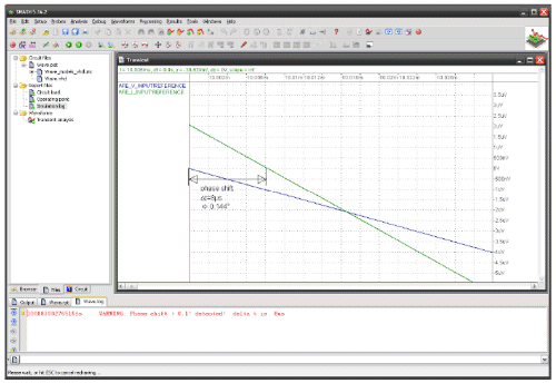
The test bench of the analog power meter part is shown in Figure 5. One can see the input range detectors D1 and D2, which observe the input voltages of the AFEs. Also shown is D3, which observes the phase shift between the two AFE channels (voltage and current). To have a power meter which complies with the standards, the extra phase shift must be compensated if it is higher than 0.05°, which is equivalent to a time offset of 2.778us. Figure 6 shows the transient simulation zoomed in to show the phase difference, which is 0.144° with an equivalence time offset of 8us. The detector warning shown at the bottom pane of the simulator reliably announces that this value is above the specified level.
Figure 5: Use of detectors to check the input range and phase shifting of a power meter design example.
Figure 6: Transient simulation, zoomed in phase shift
7. SIMULATION OVERHEAD
Adding models to the design raises the question of the impact on the simulation time. Of course, this depends strongly on the number of detectors, the computer and the simulator. In this case, release 5.17.01 of Dolphin Integration simulator SMASH is used. In the following, 8 detector elements are used in a SPICE circuit with the below listed elements:
- Parameter(s): 188
- Subcircuit(s): 18
- Capacitor(s): 118
- Diode(s): 4
- MOS transistor(s): 153
- Resistor(s): 94
- Voltage source(s): 15
- Current source(s): 2
The transient simulation of the circuit with detectors takes about 5 % more time than the simulation without detectors.
Since it is difficult to estimate the time used by designers to observe all signals and to compare that time with the detector based verification run, the focus will be set on the quality of the performed verification: significantly more important than the saved time, the detectors, in opposite to a designer, always detect unfailingly deviations from the specification!
8. CONCLUSION
It has been shown that with the use of the proposed methodology, the designer is able to create and compose specification rule checkers (detectors) by using the parameterized fundamental elements. Critical design parts can be observed continuously. During simulation, the detectors reliably check whether the design operates in its specifications and raise exceptions otherwise. Consequently, the verification phase can be automated to avoid error prone manual analysis of waveforms.
The compliance of the design specification, and therefore the overall functionality of a circuit, can be totally observed with dedicated detectors. This increases the comprehension of the design and of the influence of certain design parameters on the functionality of the circuit, thereby increasing design robustness. The use of detectors in simulation allows the identification of design defects early in the design process and therefore provides the means to reduce and even remove design iterations.
All these features increase designer's productivity and ensure design security through an accelerated automatic checking and reporting of important events in a hierarchical design flow. Since the detectors are implemented in a standardized HDL, they guarantee the compatibility of separate application schematics with different simulators and minimize efforts in creating and embedding specification rule checks independently of the overall test bench.
9. OUTLOOK
Detectors offer diagnostic support in several fields, see Figure 7.
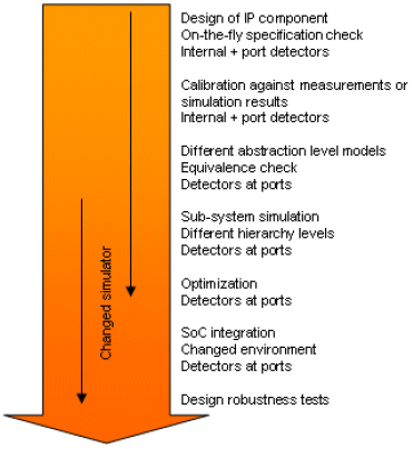
Figure 7: Detector support through the design flow
For mixed-signal circuit design, detectors can be placed at internal nets to observe specification violations. Multi-level model calibration is supported by the detectors through using a sequencing method to adapt model parameters to converge to measurements or simulations on lower levels.
Circuit optimization is improved while using the detectors with a sequencing method to optimize circuit parameters.
Design robustness tests can be enhanced through the use of detectors with a sequencing method to ensure that the Silicon IP stays in its specification.
Circuit transfer efforts can be reduced through providing virtual sockets with detectors on Silicon IP ports to observe if specifications are met in a changed environment independently from simulator.
Equivalence checking provides the possibility to check the equivalence between two models of the same or different levels of abstraction and two models of the same or different languages while applying detectors at the model interfaces (ports).
10. ACKNOWLEDGEMENTS
The first release of the detector library was developed and partly co-financed in the frame of the EU supported, regional funded project EMSIG (Development and transfer platform for the industrialization of mixed-signal circuits, FKZ 005-0604-0020).
11. REFERENCES
[1] Zhiwei Wang Abbasi, N. Narayanan, R. Zaki, M.H. Al Sammane, G. Tahar, S. “Verification of analog and mixed signal designs using online monitoring”, Mixed-Signals, Sensors, and Systems Test Workshop, Scottsdale, AZ, June 2009
[2] Ghiath Al Sammane, Mohamed H. Zaki, Zhi Jie Dong, Sofiène Tahar. “Towards Assertion Based Verification of Analog and Mixed Signal Designs Using PSL”. In Proceedings of FDL'2007. pp.293~298
[3] A. Jesser, S. Lämmermann, A. Pacholik, R. Weiss, J. Ruf, W. Fengler, L. Hedrich, T. Kropf, W. Rosenstiel. "Analog Simulation Meets Digital Verification - A Formal Assertion Approach for Mixed-Signal Verification", The 14th Workshop on Synthesis And System Integration of Mixed Information Technologies (SASIMI'07), Sapporo, Japan, pp. 507-514, Oktober 2007
[4] D. Dammers, C. Domingues, D. Schollän, L. M. Voßkämper, “Mixed Signal System Design Verification Accelerated With Detector-Based Diagnostic Method”, BMAS - 2009 IEEE International Behavioral Modeling and Simulation Conference, September 17-18, 2009, San Jose, California, USA
[5] Dammers D., Binet P., Pelz G. and Voßkämper L.M., “Motor Modeling Based on Physical Effect Models”, IEEE International Workshop on Behavioral Modeling and Simulation (BMAS), October 10-12 2001, Santa Rosa, California, USA
[6] Henry Chang, Ken Kundert. “Introduction to Analog Verification”. Based on “Verifying All of an SOC – Analog Circuitry Included”. IEEE Solid-State Circuits Magazin vol. 1, issue 4, in Fall 2009.
1 Single kernel, mixed-signal and multi-language simulator from Dolphin Integration
Related Semiconductor IP
- NPU IP Core for Mobile
- NPU IP Core for Edge
- Specialized Video Processing NPU IP
- HYPERBUS™ Memory Controller
- AV1 Video Encoder IP
Related White Papers
- FPGA based Complex System Designs: Methodology and Techniques
- Mixed Signal Design & Verification Methodology for Complex SoCs
- Reusable Test-Case Methodology for SoC Verification
- Efficient methodology for verification of Dynamic Frequency Scaling of clocks in SoC
Latest White Papers
- Transition Fixes in 3nm Multi-Voltage SoC Design
- CXL Topology-Aware and Expander-Driven Prefetching: Unlocking SSD Performance
- Breaking the Memory Bandwidth Boundary. GDDR7 IP Design Challenges & Solutions
- Automating NoC Design to Tackle Rising SoC Complexity
- Memory Prefetching Evaluation of Scientific Applications on a Modern HPC Arm-Based Processor
