Mixed-Signal IP Design Challenges in 28 nm and Beyond
Brent Beacham, Paul Hua, Cameron Lacy, Michael Lynch, Dino Toffolon
Synopsys Inc.
Abstract
This paper presents some key concepts necessary to design and build high-quality, mixed-signal IP in 28-nm or smaller geometries. The paper addresses specific design, layout, and verification techniques to address challenges posed in 28-nm technology nodes. Specifically, the paper focuses on three main areas where 28-nm technologies pose some unique challenges, Low-Power Design, Restricted Design Rules, and Design for Yield. Several design examples are presented, highlighting key techniques employed in the Synopsys® DesignWare® Mixed-Signal Intellectual Property portfolio.
Introduction
As processes continue to scale aggressively, deep sub-micron, mixed-signal design is becoming more challenging—especially when attempting to produce high-quality, high-speed mixed-signal intellectual property (MSIP). Specifically, 28 nm poses some unique challenges not found in 65-nm and 40-nm technology nodes. Section I discusses low power challenges found in 28-nm nodes and specifically addresses issues associated with the aggressive scaling of the core supply voltages in these technology nodes. Section II focuses on restricted design rules and how they have created a paradigm shift in the way circuits are designed and laid out in 28-nm nodes and some techniques to maximize design and layout reuse. Section III discusses design for yield challenges encountered in 28-nm nodes and verification methodologies to ensure robust and manufacturable IP. The issues and concepts applied in this paper have been used extensively in the Synopsys® DesignWare® Mixed-Signal Intellectual Property portfolio including the USB 2.0 PHY, USB 3.0 PHY , PCI Express®, SATA, and XAUI.
I. Low-Power Challenges
Power is one of the most important factors in defining quality MSIP. Thus, the lowering of power consumption must be considered early in the design phase. The following examples demonstrate several methods and architectures used in MSIP to minimize power both in active and sleep/low-power modes.
Multi-Vth Design Approach
Historically, for portability of IP between foundries and between processes, standard-Vth (SVT) devices are typically used. However, recent challenges in 28-nm nodes, such as corner spread, reduced supply voltages and leakage current reduction necessitate the use of low- and high-Vth (LVT, HVT) devices to maximize performance.
Corner spread is defined here as the change in circuit performance from best case to worst case device models as well as over temperature and voltage conditions. In general as the feature size decreases the output frequency for a given ring oscillator structure increases from node to node. This is shown in Figure 1, which plots a sample ring-oscillator frequency vs. technology node for 65, 40 and 28nm processes from two different foundries. As one can see from the figure, the corner spread due to global device variation is much wider in 28nm despite its typical corner output frequency being faster. This corner spread can now make it much more challenging to meet circuit specifications across all corners, especially extremes such as the inverted-headroom corner; where supply voltage is lowered by 10% and the operating temperature is -40ºC.
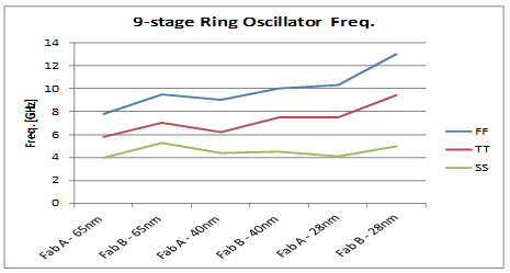
Figure 1 - "Process Spread" in 9-stage Ring Oscillator Frequency across foundry and process nodes
To combat this increased variation in circuit performance due to process and corner spread, other factors in the design (such as power supplies) can be more tightly controlled through regulation or tighter specifications. Additionally, selective use of LVT devices can also mitigate large changes in performance over corners. This is shown in Figure 2 where comparator sensitivity is plotted versus supply voltage and versus temperature for circuits implemented with SVT versus LVT devices. While performance under typical conditions is similar, LVT circuit performance degrades less at extreme voltage and temperature conditions. LVT devices also have the advantage of being able to operate under reduced supply voltages and have less mismatch due to their larger overdrive voltage. LVT however, has the drawback of increased leakage; therefore, restricted use of LVT is generally advised.
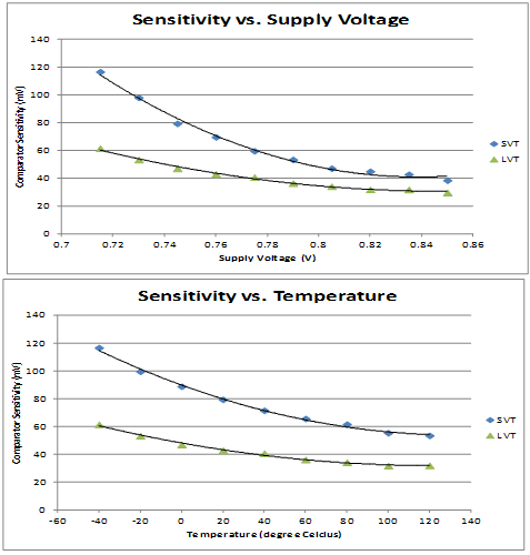
Figure 2 - Corner Spread in comparator sensitivity vs. temperature and supply voltage
HVT devices can also be leveraged to reduce static/leakage power in circuits that do not operate at the highest clock rates. In G processes, HVT devices can be used to place-and-route digital portions of MSIP as well as in combinatorial glue logic and custom-placed digital circuits within the analog portions of MSIP.
Supply Collapse Circuit Tolerance
To achieve further power savings during low-power/sleep states, especially in mobile applications, on-die core power supplies are either partially or fully collapsed. In the case of partial collapse, it is important that the internal registers still maintain their states, so that IP operation can resume when the power supply is raised. For either full or partial core supply collapse, the IP must be brought into a “known-safe state”. This is can be done by utilizing a core power supply detection circuit. When the core power supply drops below the nominally expected value, a control signal is sent to all core-to-IO level shifters. This control signals forces the level shifters into a bypass mode where a known-safe state is propagated to the circuitry being controlled.
In the case where core supply is collapsed but I/O supply is still present, circuit checks must be performed to catch unintended leakage/forward-bias paths from the I/O to core supply rails. These paths will reduce potential power savings and in the worst case can lead to high-current damage due to forward-bias currents that are larger than devices or metals can carry.
Low-supply-tolerant circuit architectures
Power reduction is often addressed through the reduction of supply voltages at the process definition level. At the 28-nm node, the core supply voltage is frequently below 1 V, and I/O supply is either 1.8 V or even 1.5 V. Consequently, significant power savings (> 1.5x) can be achieved if circuits can be designed to operate from the core supply. However, there are circuits that cannot tolerate the core supply with its elevated noise levels due to digital circuitry or supply tolerance and therefore must be regulated.
NMOS regulator output stages have the advantage of low output impedance and high power supply rejection. Unfortunately, these regulators cannot be reliably implemented with I/O supplies of 1.8 V or lower, necessitating a switch to PMOS low-drop-out (LDO) output stages. However, these regulators also suffer from higher output impedance and reduced power supply rejection—requiring that additional circuit techniques such as the super-source-follower [1] to be used.
Other design techniques to optimize power involve the use of novel transmitter architectures, such as voltage mode drivers that have a theoretical power efficiency four times that of a current mode driver. However, voltage mode drivers suffer from the restriction that peak-to-peak launch amplitude is limited to the available supply range. At 28 nm, nominal core supply voltages are frequently 0.9 V or lower, while many SERDES specifications require launch amplitudes of 0.8–1.2 Vppd. When supply tolerances of 5–10% and package loss of 1–2 dB are factored in, it is likely that the transmit launch specifications cannot be reliably met by a core-only voltage mode driver. I/O devices can be used within the transmitter, but achievable data-rates and edge-rates degrade, and jitter increases due to required level-shifters in the clock/data paths. Core devices can be overdriven, but these models are not widely available, circuit lifetime will decrease, and even a 10% overdrive does not completely negate the aforementioned supply tolerances and package losses.
An alternative approach to efficient high-swing, low-supply transmitter design is to implement a hybrid-mode transmitter that makes use of elements from both a voltage and current-mode driver. These hybrid mode output stages are used extensively in Synopsys’s high-speed SERDES IP portfolio and maximize power efficiency while still providing for swings that exceed the nominal core supply voltage.
II. Restrictive Design Rules
In 28-nm processes, the design rules are becoming much more complex in terms of device usage, density requirements, and physical design rules. These restrictions have a significant impact on device selection as well as physical implementation of the circuits in the layout. The following section discusses some of these new rules and restrictions and some techniques to address them.
Restricted Physical Design Rules
Double-pattern lithography and metal gate technologies have led to increasingly strict design rules. Poly and metal density must be kept very uniform across the die in order to reliably fabricate minimum gate length (Lmin) devices and to avoid dishing effects after interlayer polishing. The minimum and maximum poly density limits are now more tightly specified, and the checking windows have continued to decrease in size. In some cases, there are also rules for the maximum poly area per device finger. Although these rules can be challenging for digital circuits, they most strongly affect analog circuits where large devices are used for matching or as decoupling and filtering capacitors. These high-gate area devices must be fragmented and distributed to satisfy density rules. Therefore, the area for some analog circuits increases when migrating to 28 nm. Figure 3 shows a PLL charge-pump and loop filter from 40-nm and 28-nm nodes. Because of the large amount of filtering capacitance used and the restrictive density rules, the block area increased by 10%.
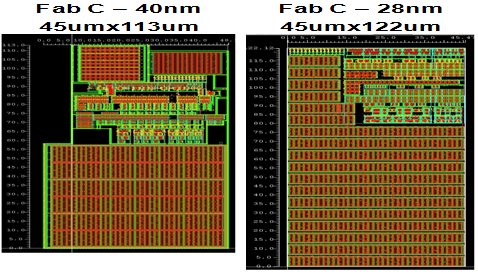
Figure 3 – Example area increase due to poly density rules
Double-pattern lithography also requires that device gate orientation be uniformly oriented across the wafer. This requirement was mostly optional at the 40-nm node, and IP blocks were generally rotated in 40-nm nodes without restriction. However, in 28 nm device and/or IP rotation is strictly prohibited. MSIP typically provides interface functionality between the chip and the outside world; therefore, MSIP is typically placed on the periphery of a die either on the N/S or E/W edge. Before unidirectional poly rules, these two placements could be satisfied by rotating a single IP GDS. Given that rotation of core-devices is no longer an option, now IP naturally has a preferred and non-preferred chip edge. Dual chip-edge support can be accomplished via translation, re-layout, or intelligent sub-block design.
Translation involves moving IP from one edge to the other without rotation. For IP that is normally on the N/S die edge, this translation means that its intended beachfront is no longer along the die edge when placed along the E/W edge. This consequence presents a challenge for flip-chip designs where bump maps and RDL patterns must change and for wirebond designs where RDL and upper metals must be used to connect the IP I/O’s to the wirebond pads at the edge of the die. While possible for smaller IP blocks, for larger IP (e.g., four-lane SERDES), it is not possible to support these placements, because routing parasitics become too large and/or IP side-edge dimensions become incompatible with pad structures on the die edge. Therefore, this translation limits the available IP configurations that can be placed on both N/S and E/W die edges. Equally sub-optimal is the complete relayout of IP to support the non-preferred chip edge, essentially creating two separate IP cores and reducing design and layout reuse, which is one of the pillars of IP design.
An efficient approach to dual-edge support is to co-design the N/S and E/W floorplans to maximize reuse of sub-block layouts, as shown in Figure 4. Sub-block aspect ratios are kept as close as possible to 1.00, and relative placements within both the N/S and E/W floorplans are kept constant.
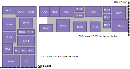
Figure 4 - Co-floorplanning of N/S and E/W IP
Restricted Device Availability
As process geometries have become smaller, the types of devices and device geometry have become more restrictive. In 130-nm nodes and above, 3.3 V transistors are generally available. In processes of 40 nm and below, often only 1.8 V I/O devices are available.[2] This limitation poses a challenge when I/O levels over 1.8 V are needed, for example, in USB 2.0 full- and low-speed signaling. To use 1.8 V devices with 3.3 V I/O levels, circuit techniques such as cascading or stacking transistors can be used to prevent a single device from “seeing” more than 1.8 V across any of the gate-drain, gate-source, or drain-source junctions.
In 28-nm and below processes, the device availability is becoming more restrictive. Restrictions can take the following forms:
- Maximum transistor gate area
- Maximum transistor W or L
- Only a limited set of transistor W and/or L’s available (“binned” devices)
Restrictions in the devices that are available set a maximum limit on the total transistor area. This limit sets the minimum random variation possible for a single transistor. This variation might exceed what is permitted for proper circuit operation. One possible solution is to change circuit architecture to one that uses digital calibration or additional control to correct the mismatch. This solution has the disadvantage of increased circuit complexity. A second possible solution is to use a combination of smaller series and parallel transistors to create an effective larger transistor, as shown in Figure 5. This constant gate area scaling approach has the benefit of achieving improved matching without changing circuit architecture or using more complicated circuitry. This approach does have a disadvantage of using a potentially large additional area due to the additional source/drain diffusion areas and interconnect needed.
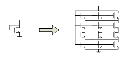
Figure 5 - Example of constant gate area remapping into technology with restricted Max W and L
III. Design for Yield
Designing high yielding IP in 28-nm nodes requires acute awareness of the process performance both from a design perspective and from a manufacturing and reliability perspective. This section focuses on some specific issues to take into account to ensure robust and manufacturable IP.
Electromigration
Electromigration is the gradual movement of metal atoms due to the momentum transfer between conducting electrons and the metal. Electromigration reduces the reliability of the IC, because over time a failure in the interconnect can occur. As metal stacks continue to get thinner and the current handling capability of the thin metal stacks decreases, satisfying EM constraints is becoming more difficult for 28-nm and smaller designs.
CustomSim® Reliability Analysis is used to simulate EM in both power and signal nets under various operating conditions. The simulation highlights nets in the layout with different colors depending on how close the current densities are relative to the process limits. The simulator enables you to quickly identify areas where EM can be a problem and to make necessary layout updates. For example, Figure 6 shows a predriver stage that has electromigration violations highlighted in red.

Figure 6 - Full chip EM plot
As design geometries shrink, metal thickness is also decreasing. The metal stackup is optimized for local signal routes at the lower levels, longer signal routes at the middle levels, and power routing at the top levels. The lower levels of metal will trade-off reduced thickness for smaller width and spacing to maximize the routing density of the interconnect. The highest metal levels are reserved mainly for power bussing and will maximize thickness while minimizing IR drop. Due to cost, minimization of the number of total metal layers is a driving factor for many designs. This factor reduces availability of the thick metals and poses challenges in providing the required current to each circuit while at the same time minimizing EM and IR drop. It is important to perform initial circuit layout with EM in mind. This correct-by-construction approach can greatly reduce the amount of iteration required to fix EM errors in the design, but manual reviewing of layout is no longer sufficient to guarantee robust IP.
NBTI, PBTI, HCI and TDDB
With CMOS process scaled down to 28 nm or lower, reliability checks are now part of the design process. NBTI, PBTI, HCI, and TDDB, which used to be second or even third-order effects, are now becoming a major failure mechanism if chip design does not consider these effects.
HCI occurs when a short channel device experiences a large lateral electric field across the drain and source. Hot carriers in the channel collide with crystal atoms near the drain area, this impact ionization creates additional carriers that can be scattered toward and trapped by the gate oxide, causing a shift in Idsat [3].
HCI failure mechanism is modeled as mean time to failure (MTTF), which is also called device lifetime, and is shown in the following equation.

As we can see from the equation, the lifetime is a strong function of device geometry, temperature, and Vds. In the Synopsys DesignWare USB 3.0 PHY, whenever possible, cascoded design structures are used to reduce Vds. Device bias checks are run in all modes and operating conditions to ensure there are no overstressed junctions in the design. The BIASCHK feature in HSPICE® checks all bias voltage (Vds, Vgs, Vgd, Vgb) during transient simulations. A report can be created to indicate whether certain bias voltages exceed a predefined limit and for a certain duration. This information can then be used to modify the design accordingly and fix the stress issue.
NBTI occurs under negative gate bias conditions and is generally modeled as a Vth shift. NBTI predominantly affects PMOS devices. Mobility of PMOS devices is significantly decreased by negative bias stress, especially under high temperature.
PBTI starts to be a design concern in 28 nm and below. PBTI affects NMOS devices under positive gate bias stress. Logic circuits can suffer from drive strength reduction, and analog circuits can suffer from mismatching due to Vth shift.
NBTI and PBTI failure mechanism is modeled as MTTF, also called device lifetime, as shown in following equation.

In differential structures, if there is no other way to limit Vgs, then it is always designed to make sure the matched devices are under the same NBTI/PBTI stress. Figure 7 shows an example of a receiver unit where the inputs are switched to a common mode voltage in Sleep mode. By design, the input stage is biased in the same condition even in Sleep mode and therefore under the same stress if there is any. In the meanwhile, the Vgs is well controlled within limits.
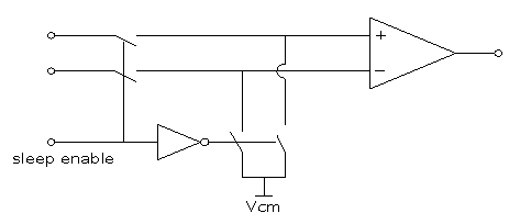
Figure 7 - Synopsys DesignWare USB 3.0 PHY Receiver
Time Dependent Dielectric Breakdown (TDDB) is a phenomenon where the oxide underneath the gate degrades over time under stress. A high-gate voltage induces a high vertical electrical field in the gate oxide, which increases the tunneling of carriers from the channel into oxide. Defects in gate oxide trap the carriers. Over time, these trapped carriers build up until a conducting path is formed, causing gate breakdown. TDDB shows a shift of threshold voltage or Idsat over time until a large increase in gate leakage and permanent damage occurs. To combat TDDB failure, careful control of on-chip biasing and supply voltages is required, and rigorous simulations using bias-check flows are critical.
Despite employed design techniques, device stress and degradation cannot be avoided entirely. Device degradation over time and design performance after years of operation can only be predicted by reliability simulations. MOS Reliability Analysis (MOSRA) in HSPICE® can be used to verify design specification over time.
Figure 8 and Figure 9 show some example MOSRA simulation results, which show aging of circuits over time. Figure 8 illustrates how the inverter delay changed after 10 years of operation, and Figure 9 shows the aging of a ring oscillator structure over time. Synopsys employs extensive use of end-of-life simulations to understand how the IP ages over time and to ensure robust operation during the life of the product, which in some cases can exceed 100 KPOH.
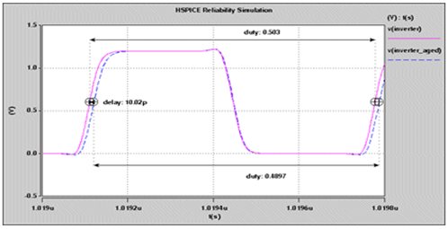
Figure 8 - Inverter Output Before and After Aging
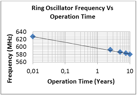
Figure 9 - Ring Oscillator Frequency vs. Time
Mismatch
In deep submicron designs, especially 28 nm and lower, device local variation has become a significant part of the total variation, as illustrated in Figure 10. With minimum feature size getting smaller, the manufacturing variants, such as gate length variation, diffusion variation, edge roughness, and doping variation, all contribute as local variation. The local variation introduces statistical mismatch, which can be covered only in Monte Carlo (MC) simulation.
In addition to the random local variation, layout dimension effect becomes so severe that designers must understand all these effects to be considered in layout phase in order to reduce design iterations. Typical layout dimension effects (LDE), which generate systematic mismatch, includes OD spacing effects (OSE), poly spacing effects (PSE), well proximity effects (WPE), and shallow trench isolation effects (STI).
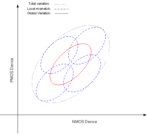
Figure 10 - 28nm device model variation
Systematic Mismatch
As previously above, OSE, PSE, WPE, and STI are the main LDE effects that introduce systematic mismatch. PSE requires matched devices to have the same poly spacing. OSE requires that matched devices have the same OD distance to surrounding devices.
STI is a mechanical stress phenomenon that causes systematic variation in device mobility and threshold voltage. The variation is a function of spacing between the edge of the diffusion and the gate and affects PMOS and NMOS differently.
There are some layout approaches that are used to reduce the effect of the STI. Figure 11 shows one technique that adds dummy devices on the outside of the active devices. This technique reduces the stress “seen” by the active device in the middle of the diffusion and reduces the Idsat variation in the device.

Figure-11 STI stress plot for NMOS and PMOS devices
WPE is another major source of device dimension-sensitive systematic variation. Due to the scattering of dopant (N-type and P-type) ions during the implant stage, the devices located near the edge of photo-resist have a different dopant density and therefore, a different threshold voltage than devices placed further away from the edge.
Besides understanding these effects and rigorously reviewing layout, to properly verify the design, final design data should be based on the simulation with a layout parasitic extracted (LPE) netlist that includes all these effects. The final result of this extensive simulation flow is a clear picture of the IP's performance over PVT including random/systematic variation effects.
Random Mismatch
Random mismatching can be evaluated only by circuit analysis and verified by extensive Monte Carlo simulations. While in general, random mismatch is inversely proportional to the devices' dimensions, mismatch also depends on the circuit itself and the parameter for which the variation is to be minimized. For example, the current mismatch of the simple current mirror shown in Figure 12 can be expressed in the following equation:
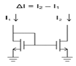
Figure - 12 Current Mirror Mismatch

Where,
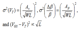
Therefore, for a given area (W * L), mismatch is minimized by increasing the length (L) of the devices. Obviously, the optimal matching comes at the expense of reduced headroom of the current mirror. For complex circuits, Monte Carlo simulations are often used to determine the critical device dimension to be optimized for reduced variability.
IV. Conclusion
This paper highlighted some key and unique challenges posed when designing mixed signal 28 nm IP. The paper also presented some techniques to address these challenges, which can be extended to deeper sub-micron technologies, such as 20 nm and 14 nm, in the coming years. The techniques outlined in this paper to address the low power, restricted design rules and yield challenges are used extensively throughout the Synopsys® DesignWare® Mixed-Signal Intellectual Property portfolio.
References
1. Hazucha, P. and Karnik, T. and Bloechel, B.A. and Parsons, C. and Finan, D. and Borkar, S., “Area-efficient linear regulator with ultra-fast load regulation”, IEEE Journal of Solid-State Circuits, vol. 40, no. 4, pp. 933-940. April 2005.
2. Euhan Chong, Nelson Lam, Navraj Nandra, Zhinian Shu, Dino Toffolon. “Building High-Quality, Mixed-Signal IP in 65-nm and Beyond “ Design Reuse Conference, 2007.
3. Rakesh Vattikonda, Yansheng Luo, Alex Gyure, Xiaoning Qi, Sam C. Lo, Mahmoud Shahram, Yu Cao, Kishore Singhal, Dino Toffolon: A New Simulation Method for NBTI Analysis in SPICE Environment. ISQED 2007: 41-46
Related Semiconductor IP
- 1.8V/3.3V I/O Library with 5V ODIO & Analog in TSMC 16nm
- Analog Switch, 100 Ohm Typical - HHGrace 110nm
- Analog MUX, Switch Resistance is around 100 Ohm - HHGrace 110nm
- Real-Time-Clock Analog, Include 32K XOSC, Capaless LDO, POR, VDT - TSMC 28nm
- Real-Time-Clock Analog, Include 32K XOSC, Capaless LDO, POR, VDT - TSMC 28nm
Related White Papers
- Integrating VESA DSC and MIPI DSI in a System-on-Chip (SoC): Addressing Design Challenges and Leveraging Arasan IP Portfolio
- Emerging Trends and Challenges in Embedded System Design
- The Growing Imperative Of Hardware Security Assurance In IP And SoC Design
- Bigger Chips, More IPs, and Mounting Challenges in Addressing the Growing Complexity of SoC Design
Latest White Papers
- Ramping Up Open-Source RISC-V Cores: Assessing the Energy Efficiency of Superscalar, Out-of-Order Execution
- Transition Fixes in 3nm Multi-Voltage SoC Design
- CXL Topology-Aware and Expander-Driven Prefetching: Unlocking SSD Performance
- Breaking the Memory Bandwidth Boundary. GDDR7 IP Design Challenges & Solutions
- Automating NoC Design to Tackle Rising SoC Complexity