Die-level process monitor for mixed signal designs
Ridgetop Group, Inc. - Tucson, AZ, U.S.A.
www.Ridgetop-Group.com
Abstract:
Designers rely on the accuracy of Process Design Kits (PDK¡¦s) for their IC designs. This paper describes independent verification of the PDK accuracy using a low-cost Die Level Process Monitor (DLPM) that can be added to a host design as an easily-implemented IP Block.
The design margins for mixed signal designs depend significantly on process parameters and their distribution across the wafer, within a wafer lot and between wafer lots. This is especially relevant for mismatch. Semiconductor foundries use in-line process monitors at the wafer level to control these parameters within a specified range. However, fabless companies and chip designers lack the access to this data, since it is kept inside the foundries. They must rely upon Process Design Kits (PDK¡¦s) for this information, and there are problems that can arise.
Therefore we propose a new methodology for monitoring critical process parameters at the die level. A small monitoring circuit is located on the same die as the host circuit, thus insuring that the sample provides an accurate representation of the devices on the chip. This is referred to as a Die Level Process Monitor (DLPM). Such monitor cells can be used to obtain the mean and the standard deviation of the most important parameters, such as threshold voltage. This is needed especially for mixed signal designs where device mismatch can create yield problems. The benefit of the new method is that the data can be accessed on each die at any time during the processing and manufacturing chain, even in the field. The circuits are very small and can be easily accessed through a simple analog pin-out or a standard JTAG interface.
MOTIVATION
The performance of analog CMOS integrated circuits depends heavily upon the foundry¡¦s ability to fabricate transistors with matched electrical behavior. Random variations inherent to the fabrication process steps result in die-level variations between transistors designed to be nominally identical. This impedes the ability of the designer to achieve exact voltage, current or charge ratios. The ¡¥mis-match¡¦ resulting from process variations is a limiting factor for both analog and digital IC¡¦s including analog signal processing systems, reference sources, multiplexed systems, digital-to-analog converters, digital memory read/write circuits, as well as the voltage margins of RAM cells [1]. Mismatch causes threshold voltage variations between nominally identical CMOS transistors.
Mismatch is inversely proportional to the area of the transistor and therefore becomes increasingly important as the dimensions of transistors are reduced [1]. A circuit design that is sensitive to mismatch must therefore use larger devices than the minimum size allowed by the foundry rules.
In addition, circuit designers necessarily are obliged to account for die-level random process variations in simulations to ensure sufficient design margin to achieve high yields. Fabless designers rely blindly on the accuracy of the Process Design Kit (PDK) supplied by the foundry in accounting for the true statistical nature of the matching-dependent voltage fluctuations. However, the values in the design kit are aggregate or worst case values, and are not specific to the designer¡¦s specific fabricated lot. Measurement of the mismatch on the circuit die itself would be useful in validating the simulations of the design margin and allow for rapid problem identification if things have gone wrong (in the design or at the foundry).
A Die-Level Process Monitor (DLPM) has been developed to measure process-related random variations in threshold voltage (VT) of CMOS transistors. The DLPM is an unobtrusive, stand-alone, IP Block designed to accurately and precisely measure the variation in threshold voltages resulting from the randomness inherent to processing. Both the absolute value and mismatch of VT are obtained.
This paper provides a general background analysis of the physical cause and effects of die-level threshold voltage variation and why it is important. The design of a reusable IP Block containing the DLPM circuit for independent VT variation measurement is described. A discussion of the implementations and benefits of the DLPM follows.
ANALYSIS
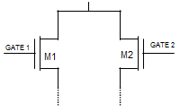
CMOS analog and mixed signal circuit designs often contain matched transistors as illustrated in Figure 1. The threshold voltage of a MOS transistor is the gate voltage required to induce a channel for current flow through the transistor.

Figure 1: Circuit example with matched transistors
Matched CMOS transistors are designed to be necessarily identical. During fabrication, the threshold voltage of a CMOS transistor is engineered during processing to a desired voltage. In a typical MOSFET process, ion-implanted charges are employed to shift the threshold voltage. This processing step, called the threshold voltage adjustment implant, is random in nature, consisting of varying energy levels of the implanted ions and subsequent temperature ramp step to diffuses the ions. The random nature of this process results in the random fluctuations in threshold voltage as a function of transistor area. Additionally, random variations in the lithography result in small geometric inaccuracies. The variation of the effective threshold voltage (![]() VT) increases as the transistor areas decrease. The relationship show in equation 1 follows Pelgrom¡¦s model [1]:
VT) increases as the transistor areas decrease. The relationship show in equation 1 follows Pelgrom¡¦s model [1]:
 (1)
(1)
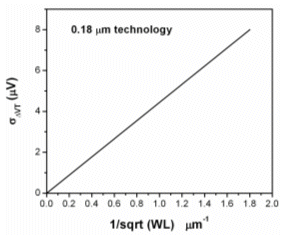
where W and L are the width and length of the MOS transistor channel area and K is a process constant supplied by the foundry in the process data sheets. It typically is on the order of 20 mV/µm depending on the process. It is evident from equation 1 that the threshold variation will increase as transistor area decreases as shown in the plotted relationship in Figure 2.

Figure 2.Standard deviation of the NMOS transistor threshold versus the inverse square root of area for a 0.18 µm process.
The DLPM circuit senses the variations in the threshold voltage related to device matching. The measured data can be used to extract die-level values of VT and ![]() VT and subsequently, the constant K in equation 1, checking the process control and accuracy of the process design kit (PDK). In CMOS analog, mixed signal and RF circuits it is the variation of the threshold voltages between two transistors rather than their absolute voltage values that is of interest for the majority of applications.
VT and subsequently, the constant K in equation 1, checking the process control and accuracy of the process design kit (PDK). In CMOS analog, mixed signal and RF circuits it is the variation of the threshold voltages between two transistors rather than their absolute voltage values that is of interest for the majority of applications.
DESIGN
The DLPM is designed to measure VT variations accurately and precisely on the die level. The DLPM is designed and biased to maximize the sensitivity of the circuit, measuring and amplifying only the ![]() VT. The DLPM design mitigates all effects known to vary VT that are not directly related to the process, including but not limited to: temperature dependence, circuit systematic offset, transistor body effects, transistor edge roughness, and fluctuations of power and bias supplier. Therefore, the DLPM directly senses the tightness of the process control. The
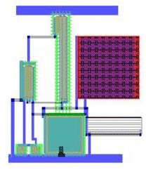
VT. The DLPM design mitigates all effects known to vary VT that are not directly related to the process, including but not limited to: temperature dependence, circuit systematic offset, transistor body effects, transistor edge roughness, and fluctuations of power and bias supplier. Therefore, the DLPM directly senses the tightness of the process control. The ![]() VT¡¦s are measured while the transistors are biased in their respective operation regime (differing between analog and digital). The DLPM meets layout constraints to ensure matched physical layout shown in Figure 3. Therefore the DLPM measured voltages and extracted statistical data can be used to verify exacting design margins for the circuit.
VT¡¦s are measured while the transistors are biased in their respective operation regime (differing between analog and digital). The DLPM meets layout constraints to ensure matched physical layout shown in Figure 3. Therefore the DLPM measured voltages and extracted statistical data can be used to verify exacting design margins for the circuit.

Figure 3: DLPM Sensor circuit layout
The DLPM is stand alone and unobtrusive, consuming little and only a small amount of power while in measurement phase (does not consume power while in off state) as listed in Table 1.
| IP Block | Power Consumption | Size |
| DLPM ƒ´VT Sensor | 100 µW | 225 µm2 |
| ADC and DAC | 40 mW | 79,000 µm2 |
Table 1: Layout properties of the monitor cells (taken for 0.5 µm CMOS process)
The design of the DLPM is quite flexible and can be applied in several different ways, depending on the power and size constrictions of the SoC (System-on-Chip) to which it is added. The most basic configuration of the process monitor consists of only the transistors and resistors associated to the sensor circuitry. This configuration results in the lowest possible power and area consumption and must be probed through an analog interface. Customer requirements permit tailored configuration of the DLPM building blocks incorporated into a specific application. Existing building blocks include the following: ![]() VT and |ƒnVT | sensors, DAC, ADC.
VT and |ƒnVT | sensors, DAC, ADC.
DISCUSSION
Due to the die-level statistical nature of the process-related parameters, and resulting degradation in performance of the amplifiers, designers are forced to submit non-optimal designs to the foundry. It is common for circuit designers to use transistors that are 4-5 times larger than the technology allows just to account for unknown matching variation. This sacrifices valuable ¡¥real estate¡¦ on the chip. In addition, experienced circuit designers incorporate die-level random process variations in the numerical simulations (SPICE) to ensure accurate modeling and high yields. The device models supplied in PDK¡¦s do not contain data relating to the statistical variation. Furthermore, Fabless designers rely blindly on the accuracy of the Process Design Kit (PDK) supplied by the foundry in accounting for the statistical nature of the offset voltages and for the supplied K value in equation 1.
The Die-Level Process Monitor (DLPM) can be implemented in many ways to realize the benefits. The DLPM measures parameters on the die-level, sensing variations that wafer-level sensors may not detect or account for. It requires no external equipment to measure the parameters. The DLPM is a feedback path for fabless companies to ensure Process compliance with the foundry-supplied process design kit (PDK). Therefore the DLPM can be used to calibrate parameter fluctuation models in circuit-level simulations. The extracted data can be utilized to increase or reduce circuit design margins resulting in increased yield. The DLPM can expedite problem resolution, determining whether design- or process-related. The DLPM can accelerate and reduce the number of design iterations. The DLPM is small enough to be laid out in the scribe streets of the wafer, resulting in little to no area trade-off.
The DLPM is fully customizable and scalable, and can be tailored to specific processes and technology.
The DLPM can be implemented with optional additional circuit blocks including a circuit that averages a range of ![]() VT from a given sample size of MOS transistors if desired, and an ADC and DAC.
VT from a given sample size of MOS transistors if desired, and an ADC and DAC.
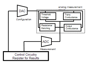
An ADC and DAC can be added to the process monitor to allow digital testing and readout through a JTAG scan bus. This standard interface offers easy access to the process monitor through 4 pins and also allows access to any other part of the ASIC if the design is integrated with the JTAG. The tradeoff for adding the ADC and DAC is increased power consumption and size. In applying the DAC and ADC a total of 1024 bytes of data are output to represent the parameter distributions, 256 bytes for each parameter as shown in Fig. 4.

Figure 4: Block diagram of full DLPM IP with optional ADC and DAC.
The die level process monitor measures the values of the transistor parameters with 2, 4 or 8 bit accuracy. Increased accuracy is available through probing of pads with an analog interface.
SUMMARY
Matching performance is a key parameter for CMOS processing. Mismatch in threshold voltage is a dominant factor in the transistor performance. The variance of threshold voltage is inversely proportional to transistor area. A novel IP Block is presented that serves the purpose of providing circuit designers with verification data to improve the accuracy of process design margins, increasing process yield, expediting problem resolution (design or process related), reducing design iterations (duration and frequency), and hastening time to market. The IP block is customizable and multiple parameter sensor blocks and data analysis blocks can be compiled as required.
ACKNOWLEDGMENT
The authors would like to thank Kaivan Borhani of Ridgetop, as well as Raj Nair at ComLSI and Brian Williams at PHYworks for their feedback and encouragement.
[1] M. J. M Pelgrom, A.C.J. Duinmaijer, A. P. G.Welbers, ¡§Matching Properties of MOS Transistors¡¨¡¦ IEEE Journal of Solid State Circuits, vol SC-24, pp 1433-1440, 1989.
Related Semiconductor IP
- ReRAM NVM in DB HiTek 130nm BCD
- UFS 5.0 Host Controller IP
- PDM Receiver/PDM-to-PCM Converter
- Voltage and Temperature Sensor with integrated ADC - GlobalFoundries® 22FDX®
- 8MHz / 40MHz Pierce Oscillator - X-FAB XT018-0.18µm
Related Articles
- Mixed-Signal Designs: The benefits of digital control of analog signal chains
- Infinite-ISP: An Open Source Hardware Image Signal Processor Platform for all Imaging Needs
- Interstellar: Fully Partitioned and Efficient Security Monitoring Hardware Near a Processor Core for Protecting Systems against Attacks on Privileged Software
- Mixed Signal SoC Applications
Latest Articles
- An FPGA-Based SoC Architecture with a RISC-V Controller for Energy-Efficient Temporal-Coding Spiking Neural Networks
- Enabling RISC-V Vector Code Generation in MLIR through Custom xDSL Lowerings
- A Scalable Open-Source QEC System with Sub-Microsecond Decoding-Feedback Latency
- SNAP-V: A RISC-V SoC with Configurable Neuromorphic Acceleration for Small-Scale Spiking Neural Networks
- An FPGA Implementation of Displacement Vector Search for Intra Pattern Copy in JPEG XS