Not all overvoltage tolerant GPIOs are the same
By Bart Keppens, Sofics | April 22, 2025
Most foundries provide GPIO libraries to their fabless customers. These libraries contain different elements like supply/ground pads, analog I/Os, digital I/Os, corner cells, filler cells, power-on-reset circuits. Frequently the foundry includes cells for different voltage domains. In 40nm CMOS the IC designer can use cells for 1.8V, 2.5V and 3.3V for instance.
Those libraries help the IC designers to create an I/O ring or I/O segments. The GPIO elements connect the inside of the chip (core) to the outside world.
The I/O (input/output) circuits have different functions
- Translate signal voltage between the core (e.g. 0.75V – 1.2V) and the outside world (e.g. 1.8V – 5V) through level shifting.
- Provide enough drive strength for output drivers to ensure the signal can reach the next chip across the board / system.
- Signal conditioning of the transients through slew rate tuning.
- Protect the core (and I/O) circuits against events like Electrostatic Discharge.
GPIO circuits have different parts
- PAD: the bondpad or bump where it physically connects to the outside world
- ESD protection: diodes, protection clamps that protect the chip circuits during Electrostatic Discharge events
- Transmit / output driver: drive signals from the inside to the outside of the chip
- Receive / input: receive signals from outside
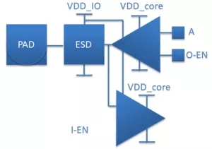
Figure 1: Different elements of an I/O circuit: Bond PAD (left side), ESD protection (diodes, clamps), Transmit circuit or output driver and receive or input circuit. In most GPIOs there are control signals to enable/disable output/input and for instance to set the drive strength and slew rate.
Transmit circuits in traditional GPIO’s on CMOS technology are designed in a push-pull configuration.
- A NMOS between I/O pad and Vss that can pull down the signal to 0 (NMOS is on, PMOS off)
- A PMOS transistor between I/O pad and Vdd that can push the signal to a high (Vdd) voltage (NMOS is off, PMOS is on)
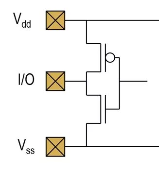
Figure 2: Typical push-pull configuration for the output driver.
Different types of (OVT) GPIOs
For some IC products the foundry provided GPIO libraries cover all the required I/O needs. However for several application types IC designers have requirements that cannot be met with those generic I/O cells. One of those requirements is the request for ‘overvoltage tolerant I/Os’. However there are a number of different cases, with distinct requirements and purposes that are all grouped under that generic name. In this article we discuss a few different cases.
Open drain
For an open drain interface the push-pull circuit is changed. The PMOS device is removed (or disabled) and only the NMOS transistor remains.
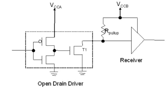
Figure 3: Schematic representation of an open drain driver. The driver consists of only an NMOS transistor. The PMOS is omitted.
The transmit circuit can basically either pull down the signal to ground or leave the signal pad floating when the NMOS is turned off. In that case other circuitry will control the signal voltage on the (shared) communication line. In a typical open drain case, there is a resistor between the I/O pad and the Vdd line. When the NMOS is off, the signal voltage will rise to the Vdd level. This approach is used for cases where multiple chips/devices connect to the same communication line. The most typical use case is the I²C interface. With just 2 lines (Data SDA, Clock SCL) system designers can create a communication network between many devices.
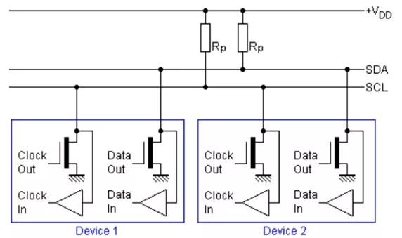
Figure 4: Simplified diagram of a I2C communication channel: Two buses are shared between different ICs: SDA for Data and SCL for Clock. Both buses are tied to Vdd through a pull-up resistance.
Because all the devices are connected to the same communication lines they all receive the signals from the other devices. It is possible that some of the devices on the bus are powered down (Vdd = 0) which means that the I/O pads can get a voltage above their supply Vdd. I²C is a ‘cheap’, 2 wires communication system where multiple devices can communicate. It is typically slower than dedicated communication for each pair of devices.
Overvoltage tolerant
The ‘Overvoltage tolerant’ requirement basically means that an I/O that normally runs at 3.3V for instance (driving, receiving at 3.3V) must be able to withstand higher voltage transients like 5V. Some people refer to this as input overvoltage tolerance. During operation the I/O voltage can be higher than the supply voltage. This affects the design of the I/O circuit because without consideration of these higher voltages it can damage the circuit. It also affects the ESD protection approach. A (parasitic) diode between I/O and Vdd will allow current to flow from a 5V signal to the 3.3V supply line, pushing the 3.3V supply to a higher voltage. Our colleagues Wouter and Koen wrote articles about this (link1, link 2).
Cold-spare
Cold spare relates to the fact that an unpowered (cold) replacement (spare) device is connected to a shared communication line. This is used a lot in space applications for instance. System designers add an identical ‘cold spare’ device that can be used as a back-up when the first circuit is damaged somehow. If the primary circuit is not behaving correctly it can be turned down and the backup circuit is powered up to take over. So both primary and secondary / back-up can be switched on/off independently. However, it is common practice to route the I/O signals to both primary and back-up circuits and thus only provide a switch for the power to select between the primary and the back-up circuit. This has an important consequence for the I/O pads. The device that is powered down still receives the signals. The I/O voltage can thus be higher than its supply voltage.
Back drive protection
Picture a living room with a TV, a tuner/recorder, a DVD player, a gaming console and a sound system. All these systems are connected with HDMI or USB cables. However the consumer does not need to power every device to enjoy entertainment. When the TV is on, the DVD player might still be turned off. But the DVD player is connected to the TV with an HDMI cable. The TV could somehow power up the chips in the DVD player through the signal lines. The voltage of the I/O pad can be higher than the supply, during a powered down mode. IC designers need to adapt the traditional push-pull approach (PMOS parasitic diode) and ESD diode up to block current from signals to the Vdd.
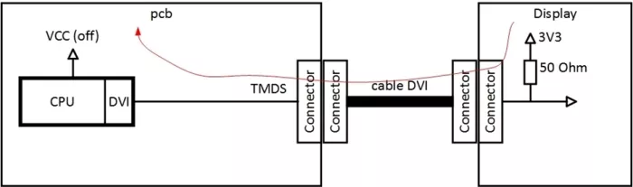
Figure 5: Back-drive protection is required in systems where one side of the communication line is powered down. without attention for this the powered device can power the other side through the ESD diodes for instance.
Hot swap / hot plug
End-users of consumer electronic appliances like computers, music players, video cameras and many other devices have the tendency to insert and remove USB, HDMI, … cables while devices are running. Suppose a user inserts a USB-memory stick (powered down) to a computer that is already operating. This could lead to signals being applied on the I/Os before the device is fully up and running. Because the total (parasitic) capacitance on the I/Os is many times smaller than the total capacitance of the power domain the power up rate of the supply is much slower. The voltage at the pad can be higher than the supply voltage during such power-up transients. Once in operation the voltage at the I/O pad typically stays below the Vdd voltage.
It could be that signal and supply voltage is beyond the maximum voltage tolerated by the I/O transistors. In that case stacking of 2 or more transistors is required to reduce SOA violations. Or or that an not-fully powered device is provoking an unwanted current drain path to the bus which corrupts the communication.
Fail-safe
Fail-safe is another concept often grouped under the umbrella of overvoltage-tolerant I/Os. The term “fail-safe” refers to the ability of a system to avoid damage or failure even when some parts of the system are powered down — a key requirement in multi-voltage or multi-device environments. In fail-safe configurations, multiple devices share the same communication lines (e.g., I²C, SPI, UART), much like in cold-spare setups or open-drain topologies. Some devices on the bus may be unpowered while others remain active and continue communication. This means that the unpowered device’s I/O pins might be exposed to signal voltages that are higher than their own supply voltage (which is 0V in the powered-down state). Consequently, the I/O circuitry must tolerate these conditions without causing latch-up or current leakage through protection diodes. Typically, the voltage at the I/O stays below the supply voltage when the device is active, so the critical condition is during power-off. This scenario mainly stresses the PMOS transistors — particularly the parasitic diode between the I/O and VDD — and the ESD structures connected between the I/O and the supply rail.
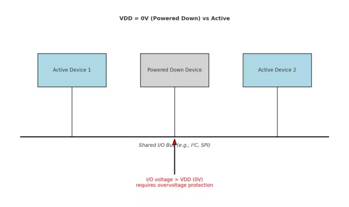
Figure 6: In a Fail-safe system it is possible to power-down some subsystems / devices connected to a shared bus without causing the entire system to malfunction (‘fail’).
Inductive load
In certain applications the output drivers of an IC are connected to coils or to devices with an inductive behavior. Inductive loads can be dangerous in fast switching circuits. The signal voltage can quickly increase by 100% if the transmitter changes state. Dual diode based protection is not tolerated because the I/O voltage can rise quickly above the supply voltage level. The large amount of current could make the supply lines noisy.
For some power management chips, IC designers use an inductor and switches to create a higher voltage than is normally available on the chip. The I/O voltage can exceed the supply voltage during such transients.
Decreasing voltage levels in advanced nodes
For designs in mature processes (0.25um and older) IC designers used 5V CMOS interfaces. For years, devices could use 5V signals to communicate. All the chips from different vendors were compatible enabling an easy system development. However that changed. Every time when newer process technology was launched the supply voltage range was reduced. This reduction was neccessary for reliability but also to reduce power consumption.
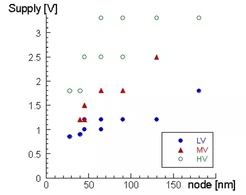
Figure 7: Supply levels for low (LV), Medium (MV) and high (HV) voltage domains across process generations between 180nm and 28nm, multiple fabs and multiple process variations
When the maximum supply voltage is reduced the I/O interfaces / protocols had to follow. In several waves we moved to 3.3V, 2.5, 1.8, 1.5 and then 1.2V signaling.
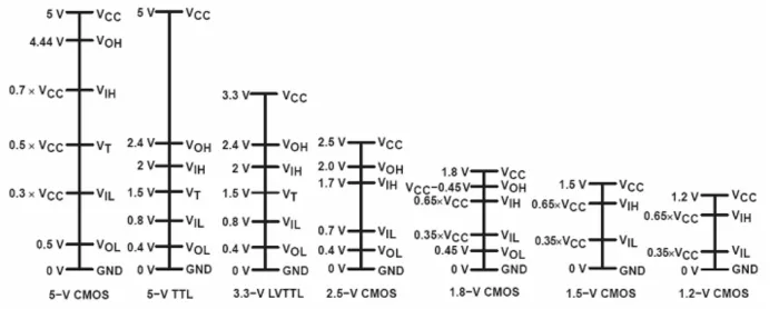
Logic threshold voltage levels for the different interface types
Sometimes it is possible to connect chips using different protocols. Two devices are compatible if the following requirements are met:
- The VOH (Output High Voltage) of the driver must be greater than the VIH (Input High Voltage) of the receiver.
- The VOL (Output Low Voltage) of the driver must be less than the VIL (Input Low Voltage) of the receiver.
- The output voltage from the driver must not exceed the IO voltage tolerance of the receiver.
Sometimes this leads to requirements that e.g. a 1.2V must be able to tolerate 1.5V signals and still operate. So the 1.2V circuit needs to be specially designed with higher tolerance.
Electrical overstress
Similar to the inductive loads the voltage on IO pins can be higher than expected during some electrical over stress situations. E.g. advanced CMOS timing circuits in LCD panels may receive a voltage as high as 17V for a long duration. In USB and HDMI applications another problem can occur. The USB/HDMI high speed data lines operate from a 3.3V supply. However there are also 5V lines in the same cable. One of the tests submitted to USB ICs is the „5V short circuit withstand‟ requirement. It is used to check if the USB data lines are damaged or degraded if they are shorted together with a powered VBUS line for 24 hours.
What are the solutions?
To facilitate these different cases IC designers need to use a different type of GPIO. For all these cases the typical (dual) diode based ESD protection cannot be used. The diode from pad to Vdd needs to be removed. In this article 6 different ESD concepts are compared.
For some of the cases the I/O circuits need to be changed as well to ensure they can handle a higher voltage. More information in these articles
Related Semiconductor IP
- On-chip ESD/EOS/Latch up protection for advanced and low voltage processes
- On-chip ESD/EOS/Latch up/EMC protection for high voltage and BCD processes
- Robust circuit and interface solutions
- General Purpose Input / Output Controller (GPIO)
- Generic GPIO controller
Related White Papers
- Times are tough all over, so don't write off the silicon foundry model just yet
- How are you planning to verify all that DfT?
- What if the IP you are looking for does not exist?
- eFPGA Saved Us Millions of Dollars. It Can Do the Same for You
Latest White Papers
- Breaking the Memory Bandwidth Boundary. GDDR7 IP Design Challenges & Solutions
- Automating NoC Design to Tackle Rising SoC Complexity
- Memory Prefetching Evaluation of Scientific Applications on a Modern HPC Arm-Based Processor
- Nine Compelling Reasons Why Menta eFPGA Is Essential for Achieving True Crypto Agility in Your ASIC or SoC
- CSR Management: Life Beyond Spreadsheets