Low Power 7T SRAM Cell Scheme - ''Saving Write Zero Power''
University Centre for Instrumentation & Microelectronics, India
ABSTRACT
This paper presents a Seven-transistor SRAM cell intended for the advanced microprocessor. A low power write scheme, which reduces SRAM power by using seven-transistor sense-amplifying memory cell, has been described. By reducing the bitline swing and amplifying the voltage swing by a sense – amplifier, which is a part of the memory cell, the charging and discharging component bit / data lines power consumption is reduced. The existing technology (6T-SRAM) is briefly discussed with their strengths and weaknesses. The design metrics for the Seven-transistor cell are discussed in detail and performance and stability are evaluated. Finally, a comparison is done between existing six-transistor technology and the proposed (seven-transistor) technology. The comparison includes power and delay.
I. Introduction
SRAM continues to be an important building block of system-on-a-chips (SoCs). The low-power feature for on-chip SRAMs is becoming more important, especially for battery-operated portable applications. It is, however, also one of the most significant challenges of high-speed VLSI circuits whose primary target is not low power but high performance. As systems become more complex toward higher performance, on-chip SRAMs tend to have a large number of bit width such as 16 to 256 or even greater. In this type of SRAM, the active power of the SRAM is dissipated mainly by charging and discharging of the highly capacitive bit/data lines, as shown in Fig. 1(a), due to their full swing nature in write cycles.
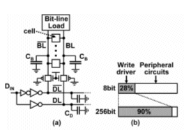
Fig. 1. Write power consumption in conventional SRAMs. (a) Capacitive load on bit/data lines. (b) Write power comparison between two different SRAM configurations.
Therefore, power consumed in write cycles is much larger than that in read cycles. Fig. 1(b) shows power estimation of 4-Mb SRAMs having two different organizations. If bit width is 8, only 28% of the total power is consumed by driving bit/data lines. When bit width becomes 256, however, this value is increased to 90%. Reducing voltage swing on the bitlines is an effective way to decrease the power dissipation in write cycles. In the half-swing (HS) scheme [2], 60% power reduction was achieved by restricting the bitline swing to a half in combination with charge recycling. It is, however, difficult to further reduce the power because of write-error problems in the HS scheme. The HS scheme also has a problem in stable read operation because precharging bitlines during read cycle increases the possibility of an erroneous flip of cell data. In fact, being different from DRAMs, half- precharging of bitlines has not been widely used in SRAMs. Therefore, precharging in read cycles must be avoided. If the bitline voltage level in read cycles is lifted up from half- in the HS technique, another issue occurs. When the write and read cycles come alternately, there is additional power consumption for bitline voltage recovery due to the mismatch of the voltage level of bitlines in read cycles and that in write cycles. In this paper, a novel small-swing SRAM scheme using a sense-amplifying cell is presented, with which further power saving in write cycles is possible. Since the write power is dominant in SRAMs with large bit width, the peak and average operation current can be reduced. The proposed scheme applies similar technique as used in the driving source line (DSL) scheme reported in [3]. Two important differences between the two schemes will be explained in later sections. This paper also has two new contributions which were not included in [2]. First, several important tradeoffs regarding the design of the source-potential control circuit are discussed in detail with SPICE simulation results.
This paper is organized into five sections. In Section II, the overall architecture of the 7 transistor SRAM cell scheme is explained with detailed circuit diagrams and operation waveforms. The difference of the proposed scheme from the DSL scheme is also explained. In Section III, quantative analysis on design tradeoffs is described with SPICE simulation results. It is also shown that these tradeoffs are governed by two design parameters. In Section IV, measurement results of the simulated cell shown. In Section V, all discussions are summarized.
II. 7 Transistor SRAM Cell Scheme
Figs. 2 and 3 show the circuit diagram and the operation waveform of the proposed cell scheme, respectively. The salient feature of the scheme is an additional nMOS connected to the source of driver nMOS transistors of the memory cell, which enables small swing of bit lines in a write operation. This additional nMOS is referred as the switch Vss in the rest of this paper. A bit line is precharged to Vdd - Vtn by an nMOS load transistor and is pulled down to Vdd – Vtn -DBL in a write “0” operation, where Vtn and DBL are threshold voltage of the load nMOS and write swing, respectively. The precharge level must not be Vdd because access transistors of the cell cannot turn on in the write operation in this scheme. There is no additional power consumption even if the write and read cycles come alternately, because there is no mismatch between the voltage level of bit lines in read cycles and that in write cycles. The source-line control signal, SLC, is synchronized with the word line signal WL, and the switch Vss is turned off before WL goes up to high in a write cycle. Even if the voltage difference between a pair of bit lines is small, the cell node can be inverted because the driver nMOS transistors do not draw current while the word line is activated, thanks to the switch.
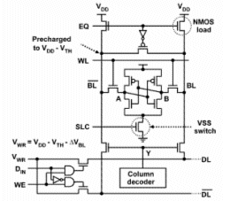
Fig. 2. Overall architecture of 7T SRAM cell scheme.
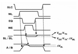
Fig. 3. Write cycle waveform.
After WL goes to low, SLC goes back to high and small-swing data is amplified to full swing inside a cell. Note that all the cells connected to the activated wordline should be written in a write cycle in this scheme. If the numbers of cells connected to a wordline and to an SLC signal line are 64 and 256, respectively, for example, data stored in 192 cells become unstable while 64 cells are written. The voltage level of Vdd-Vtn -DBL has been achieved by a dc–dc converter with a help of voltage reference generator, as shown in Fig. 4.
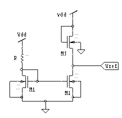
Fig.4. Write voltage generator design. (Circuit diagram.)
The converter supplies Vwr to each bitline through the write circuit. Though the voltage generator consumes static current, only one generator is required in the whole SRAM chip and its power overhead is negligible.
Both the proposed 7T and the driving source line (DSL) cell [3] achieve small-swing write operation by setting the source terminal of the cell driver nMOS transistor floating in write cycles. The main advantages of the proposed scheme over the DSL scheme are avoidance of both half- precharging of bitlines and negative voltage. In the DSL scheme, the source node of the cell driver nMOS transistor is driven to negative voltage during a read cycle in order to increase read current. This causes overstress on the gate oxide of the cell nMOS transistor and deteriorates device reliability, which becomes a more serious issue in scaled devices. Avoidance of half- precharging of bitlines, which is also used in the HS scheme, is also preferable in terms of stable write operations because the write error rate increases as the bitline voltage level decreases. Another small-swing write technique, switched virtual-GND level (SVGL) technique can be found in [3]. The difference between the SVGL scheme and ours is as follows. In the SVGL scheme, a source terminal of cell driver nMOS transistors is connected to a virtual-GND line, and its potential is increased from ground level during write cycles to achieve small swing write operation. While an SLC signal line runs in parallel with a wordline in the SAC scheme, a virtual-GND line in the SVGL
Scheme runs in parallel with a bitline. Since a bitline is usually longer than a local wordline, the overhead of driving the virtual- GND line in terms of delay, power, and area is large in comparison to those driving the SLC signal line. In addition, when the bit width is, the number of activated virtual-GND lines is equal to, while the number of activated SLC signal lines is 1. Thus, the SAC scheme can achieve lower power and higher speed than the SVGL scheme.
III. Cell Design Consideration
In the proposed scheme, the primary concern in cell design is tradeoffs among read delay, noise margin, and cell area. Before going into quantative analysis of these three issues, it is explained that the tradeoffs are tightly related to two design parameters of the switchVss: b and N
Fig.5 shows the equivalent circuit of a proposed cell in a read cycle. Along the read current path, there are three nMOS transistors stacked. They are a cell access transistor, a cell driver transistor, and the switch Vss, whose width are denoted as Wa, Wd and Wsw, respectively. By defining b as the ratio of Wsw to Wd , the first key design parameter b is obtained. With such a definition, b becomes independent of technology-specific parameters and the following discussions can be applied to every technology node. In a conventional six-transistor cell, Wd is set around 3Wa and b is virtually infinite. According to the insertion of the switch Vss having finite value, read current and static noise margin will decrease. Therefore, it is clear that larger is better in terms of read delay and noise margin, but its maximum value is strictly limited by area constraints. The second key parameter N, is related to a layout issue of the switch Vss. The switch cannot be placed cell by cell because area overhead goes beyond 20%. Therefore, it should be shared by a group of neighboring cells.
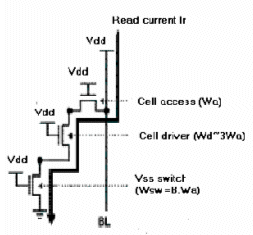
Fig. 5. Read current path of a seven-transistor cell.
In this case, there are three elements in each row which cause area penalty. They are the SLC signal line, the switch itself, and the common source line which connects each cell to the switch.. The simplest way is to set the value of to its maximum, the same as the bit width. Such a configuration is, however, impossible in practice, due to the following reason. Fig. 5 shows the read current path in the shared switch structure. When read current flows through each cell in read cycles, the maximum current through the common source line is as large as N. IR
IV. Simulated Results
A proposed 7T SRAM cell is simulated with 0.35mm CMOS process. The SRAM simulated cell operated at 100 MHz with 2-V supply. The features of the cell and the technology are summarized in Table I.
| Technology | 0.35mm CMOS |
| SRAM | 7 transistor cell |
| Supply voltage | 2V |
| Operating frequency | 100MHz |
Table 1: Cell summary
Simulated results showing the dependence of bitline power is given in fig6. Power dissipation of 232 µW in full swing write is reduced to 60mW when DBL is lowered to of 400 mV.
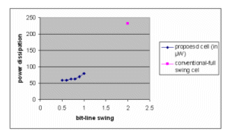
Fig 6.simulated result of power dissipation in proposed cell and conventional cell.
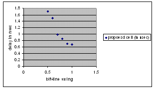
Fig 7. delay in proposed cell
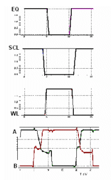
Fig 8. Simulated wave form result of proposed 7T SRAM cell
V. CONCLUSION
The 7T cell scheme is presented for wide-bit SRAMs. A simulated cell was designed in 0.35µm CMOS technology, and correct read/write operation was verified. By using the small-swing bitline scheme, 75% of power in write cycles is saved. As a guide for practical design, is shown that tradeoffs among area, delay, and noise margin are governed by two design parameters, N and b , associated with the Vss switch. Decreasing b saves layout area but degrades both noise margin and read delay. Increasing N for a given b can also saves layout area. But when electromigration effect has to be taken care off wide metal can be drawn for a common source line within a cell pitch. Assuming 7T SRAM, the delay overhead and area overhead of the scheme are estimated to be 15% and 11%, respectively. The difference between the proposed scheme and other small-swing write techniques are also discussed in detail. Two main advantages are avoidance of half- precharging of bitlines and negative voltage on cell source lines. With these advantages, the proposed scheme can save more write power without degrading cell stability and device reliability. The possibility of reducing cell leakage power during active mode by slightly modifying the 7T cell scheme has also been explored.
VI. REFERENCES
[1] Itoh, Kiyoo, Sasaki, Katsuro, and Nakagome, Yoshinobu, “Trends in Low-Power RAM Circuit Technologies”, Proceedings of the IEEE, vol. 83, pp. 524-543, april 1995
[2] K.W. Mai, T. Mori, B. S. Amrutur, R. Ho, B.Wilburn, M. A. Horowitz, I. Fukushi, T. Izawa, and S. Mitarai, “Low-power SRAM design using half-swing pulse-mode techniques,” IEEE J. Solid-State Circuits, vol. 33, pp. 1659–1671, Nov. 1998.
[3] H. Mizuno and T. Nagano, “Driving source-line cell architecture for sub-1-V high-speed low-power applications,” IEEE J. Solid-State Circuits, vol. 31, pp. 552–557, Apr. 1996.
Related Semiconductor IP
- NPU IP Core for Mobile
- MSP7-32 MACsec IP core for FPGA or ASIC
- 100G / 200G / 400G / 800G / 1.6T MACsec
- 32 bit RISC-V Multicore Processor with 256-bit VLEN and AMM
- UHF RFID tag IP with 3.6kBit EEPROM and -18dBm sensitivity
Related White Papers
- Low power is everywhere
- An ESD efficient, Generic Low Power Wake up methodology in an SOC
- A need for static and dynamic Low Power Verification
- Low Power Design for Testability
Latest White Papers
- Concealable physical unclonable functions using vertical NAND flash memory
- Ramping Up Open-Source RISC-V Cores: Assessing the Energy Efficiency of Superscalar, Out-of-Order Execution
- Transition Fixes in 3nm Multi-Voltage SoC Design
- CXL Topology-Aware and Expander-Driven Prefetching: Unlocking SSD Performance
- Breaking the Memory Bandwidth Boundary. GDDR7 IP Design Challenges & Solutions