Systematic approach to verification of a mixed signal IP - HSIC PHY case study
Dariusz Kaczmarczyk, Dariusz Pieńkowski, Marcin Sadowski, Tomasz Klimek - Evatronix SA
Harry Peterson, Mohagi / Evatronix SA
Wojciech Sakowski, Evatronix SA / Institute of Electronics, Silesian University of Technology
Abstract
This paper discusses verification process of a mixed signal core of an HSIC PHY. After explaining the specific topic related with HSIC comparison to USB, the verification strategy is shown. The strategy is explained from the top level point of view, and detailed description is covered in subsequent sections. In following sections the system level testbench and interoperability testbenches are explained parallel to local testbenches for analog block characterization. The testchip verification procedure follows this detailed description. Presented methodology is based on the robust analog and digital design flows. Usage of mixed signal simulators allows combining these flows and increases level of the verification. Additional advantage of presented strategy is the reuse of Verilog models of standard modules like PLL and JTAG controller in future projects.
Introduction
High-Speed Inter-Chip USB (HSIC) standard allows replacing USB cables and connectors with PCB traces. The HSIC transceiver is optimized for circuit board layouts, which results in significantly reduced size and power consumption compared to the standard USB PHY.
The HSIC standard supports only USB Hi-Speed (480Mb/s) bit rate and thus it requires source of the high speed clock. One of possible solutions to facilitate deployment of the HSIC PHY is an internal PLL that provides high speed clock necessary for the digital part of the PHY.
HSIC PHY – Differences vs. USB PHY
Architecture of the HSIC PHY is almost the same as the standard USB PHY. The HSIC PHY provides the same timing for USB packets and all USB events like suspend, resume signaling, remote wakeup signaling and duration of the USB reset. Functional differences are caused mainly by the fact that the HSIC connection doesn’t support hot plugging and unplugging. The HSIC standard supports only Hi-Speed and uses source synchronous 240MHz DDR signaling that replaces standard USB differential D+/D- analog lines. Maximum length of the DATA/STROBE PCB traces is limited to 10cm.
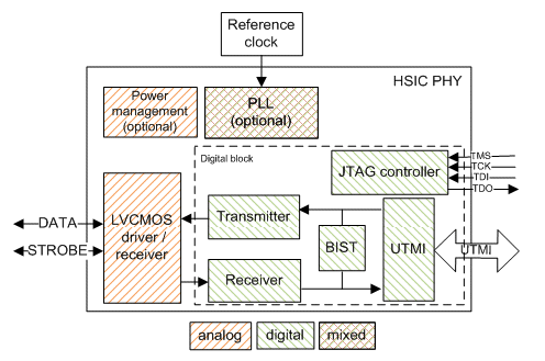
Figure 1 The HSIC PHY Block Diagram
Verification strategy
The verification strategy adopted at Evatronix is shown in Figure 2. It shows that the verification starts from Verilog model of the HSIC PHY, and ends with the same model but with analog parts as SPICE netlist incorporated into the simulations.
Subsystem verification
The HSIC PHY consists of digital, analog and mixed-signal blocks as shown in Figure 1. Since the nature of these blocks is different thus slightly different verification policy is adopted for each group of blocks. The digital block is already functionally verified at the top level, and there are no specific testbenches for this block and its components.
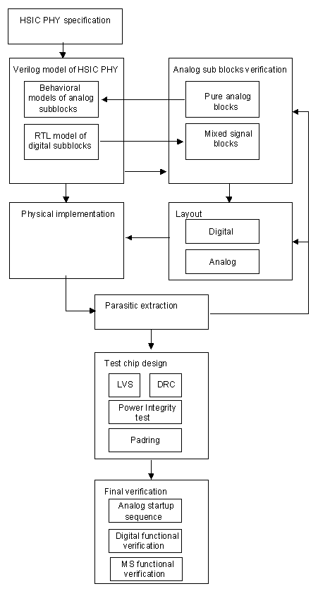
Figure 2 Verification strategy block diagram
Different strategy is applied for analog blocks (LVCMOS driver / receiver in Figure 1). These are the input buffers, output drivers and power management block required for PLL, etc. All of them are verified in analog testbenches. The stimuli for each particular testbench of the block are defined either by other analog block or by the behavioral model of the digital part. Testbenches verify parameters defined at the system level specification over voltage, temperature and process corners. These testbenches are designed to be independent of the actual process and therefore can be reused for porting to other technology nodes. In general, one particular testbench verifies more than one design parameter, and it is fully automated by an extensive use of scripting language.
As a consequence, simulation results are almost self documented and additionally a set of input parameters for Verilog model is generated. These Verilog models are then used in system level verification described later.
Mixed signal subsystems are also treated differently. Such a block is the PLL. Actually it is a mixed-signal subsystem of a larger mixed-signal HSIC PHY IP block. The verification of this subsystem takes the most time of the verification. In the design methodology the verification is a key component. Firstly the requirements for particular PLL blocks in term of phase noise, voltage gain, dead zone, PSRR, loop filter cut-off frequency and current consumption are derived from top level specification and behavioral simulations using commercial and proprietary Evatronix tools.
This step is essential since by using these tools, PLL performance can be recalculated with set of parameters already obtained from analog simulations of the particular analog block. It significantly reduces the verification time. Analog blocks inside the PLL are verified in the same way as described above. The digital blocks, such as the divider and the PLL controller are functionally verified in behavioral testbenches that use behavioral models of analog parts, like VCO, loop filter, charge pump etc. In this step the actual performance of analog blocks is ported into the Verilog models.
By porting more and more information into Verilog behavioral models of the functionality of the PLL analog blocks we reached a point that further implementation of it brings no benefits within functional verification. With proven functionality the analog verification takes place. In full analog simulations digital parts (controller, divider) are simulated at the transistor level. These simulations results are limited to transient analysis (huge complexity of the system), but allow additional functional verification, current consumption, tuning range and settling time over all voltage, temperature and process corners. To speed up the simulation and verification process checkerboard strategy is adopted. That means that not all components are simulated at transistor level from beginning at the same time, but rather more and more blocks are switched from Verilog or VerilogA models to their SPICE representations.
In general it is also possible to verify the PLL using mixed mode simulations, where digital blocks are simulated at behavioral level, and analog at SPICE level. For this particular case we found the verification speed to be sufficient and not used this technique for PLL verification, but it is used for final test chip verification.
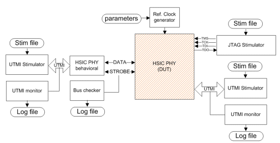
Figure 3 The System Level Testbench
Testbench architecture
The HSIC PHY is functionally verified by means of two separate testbenches – the system level testbench and the interoperability testbench.
The system level testbench has been developed to support mixed-level verification. Bus models of the UTMI and USB serial interfaces have been reused from testbenches developed for USB controllers. Test suites were developed basing on testplan covering the features that are specific for the digital part of the HSIC transceiver:
- Rx Channel (NRZI decoding, bit unstuffing, SYNC/EOP recognition, interpacket gaps, elasticity buffer overflow detection)
- Tx Channel (bit stuffing, NRZI encoding, SYNC/EOP generation, interpacket gaps)
- Bus events (power-on connection, suspend/wakeup/remote wakeup, and USB reset)
- Test modes (debug interface, BIST)
System level testbench models typical conditions that appear in a real world USB systems like:
- Reference clock frequency accuracy
- Reference clock jitter
- Size of the USB packets
- Contents of the USB packets
- Interpacket gaps
- Incorrect USB packets
System level testbench was used for pure digital simulation focused on the verification of the digital part of the HSIC PHY. Analog portions of the HSIC PHY were modelled using Verilog HDL which dramatically reduced simulation time and enabled exhaustive simulation necessary to achieve required levels of the code coverage and functional coverage.
System level testbench was used to verify interoperability of the digital and analog portions of the HSIC PHY using mixed-signal simulation.
System level testbench was used to verify timing parameters of the DATA/STROBE signals as well as timing of the UTMI interface.
The interoperability testbench is the testbench developed to verify the USB controller. It allows instantiation and simulation of the HSIC PHY connected to the USB controller. Test suite originally developed for USB controller is used to exercise the HSIC PHY.
Reduced test suite was developed to cover functionality that is necessary to ensure correct interoperability of the analog and digital parts.
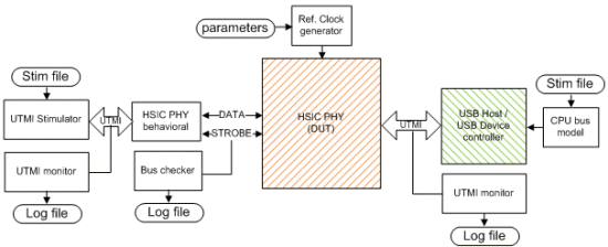
Figure 4 The Interoperability Testbench

Figure 5 Mixed-signal simulation Testbench
Physical implementation
With schematic of HSIC PHY subblocks ready the layout design starts. A good layout is a key factor of high performance analog and mixed-signal blocks. In Evatronix the layout of particular block is done mostly by the designing engineer and set of layout review meetings take place. This substantially reduces number of layout re-spins. Nevertheless parasitic extraction and simulation of backannotated netlist is done. Analog blocks are verified again and checked against their specification. The same is for PLL. Parasitics are more disturbing for subblocks working at higher frequency, especially VCO and are almost invisible for circuits working at DC.
Parasitic analysis has also important implications on power integrity inside the chip. Digital components consist of many clocked flip-flops and can in some circumstances draw significant peak supply current. This in turn adds noise to the substrate and thus affects chip performance. Additionally, it can cause voltage drops on supply rails when its resistance is not sufficient. This possible issue is also analysed. Tools used extensively at Evatronix provide such a analysis, but to be more rigorous on this issue the current consumption from digital parts is analysed in a analog dynamic environment. Layout of supply rails is made accordingly, but supply current spikes are also limited by using spike reducing techniques in the digital component architecture, as well.
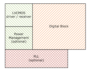
Figure 6. Floorplan
The floorplan of the HSICPHY is shown in the figure 6. Care is taken to keep chip area small without degrading the chip performance. The sensitive blocks as VCO are placed away from noisy digital part and output line drivers.
Test chip design and sign off
The testchip is only a demonstration of a working HSIC PHY IP. Additionally to the HSIC PHY it has a pad ring that enables package bonding and assures ESD protection. Finally, DRC and LVS checks of the chip are performed. Placing the chip into a package implies extensive package and board parasitic modeling in respect with power and signal integrity analysis. All IO circuits (particulary designed HSIC IO pads and IO pads taken from standard IO libraries) are modeled and simulated with parasitic extracted pad ring of the test chip. This analysis performed at SPICE level simulation enables us to arrange the pin position and bonding diagram in the way that crosstalk and voltage dependent delays caused by dynamic voltage drops are minimized.
One of the final tests in the signoff procedure is a startup sequence when the chip is powered up. This is a pure analog simulation and it consumes much time. However, this verification made within an analog testbench is performed to check power up sequence and wake up conditions for clock generators.
Finally functional verification is made in a mixed-signal simulation environment, shown on figure 5, in order to ensure correct interoperability of the real analog block with digital part. The behavioral models of the analog parts (LVCMOS driver / receiver and PLL) were replaced with the extracted SPICE netlists and simulated using fast SPICE while the digital blocks were selected as post layout digital netlist and simulated using Verilog simulator. That simulation finaly is used to verify start-up sequence and integration of the HSIC PHY within the chip together with all IO pads. In order to shorten the simulation time the Verilog representation of the IO pads is used. This technique is used for either system level verification shown in Figure 3 or for interoperability verification shown in Figure 4.
Conclusions
Presented methodology is based on the robust analog and digital design flows. Usage of mixed signal simulators allows combining these flows and increases level of the verification.
Testbench can be reused during porting the HSIC PHY to any technology. Verilog models of standard modules like PLL and JTAG controller can be re-used in future projects.
Literature
- The USB 2.0 specification released on April 27, 2000 (www.usb.org)
- USB 2.0 Transceiver Macrocell Interface (UTMI) Specification, Version 1.05 3/29/2001 (http://www.intel.com/technology/usb/spec.htm)
- UTMI+ Specification, Revision 1.0, February 25th, 2004
- High Speed Inter-Chip_1_0 final HSIC specification, Sept 23, 2007 (www.usb.org)
Related Semiconductor IP
- SuperSpeed USB 3.0 Host Controller Supporting SSIC and HSIC
- SuperSpeed USB 3.0 Dual Role Device Controller, Configurable for SSIC and HSIC
- SuperSpeed USB 3.0 Device Controller Supporting SSIC and HSIC
- USB 2.0 Hi-Speed OTG Controller Subsystem w/AHB Interface Supporting HSIC (config. as Device only or Full Speed only)
Related White Papers
- Modeling and Verification of Mixed Signal IP using SystemVerilog in Virtuoso and NCsim
- Mixed Signal Design & Verification Methodology for Complex SoCs
- High bandwidth memory (HBM) PHY IP verification
- Ins and Outs of Assertion in Mixed Signal Verification
Latest White Papers
- Ramping Up Open-Source RISC-V Cores: Assessing the Energy Efficiency of Superscalar, Out-of-Order Execution
- Transition Fixes in 3nm Multi-Voltage SoC Design
- CXL Topology-Aware and Expander-Driven Prefetching: Unlocking SSD Performance
- Breaking the Memory Bandwidth Boundary. GDDR7 IP Design Challenges & Solutions
- Automating NoC Design to Tackle Rising SoC Complexity