High-Speed Serial fully digital interface between WLAN RF and BB chips
Sophia Antipolis, France
Abstract :
This paper presents a new interface between the two main chips typically found in Wireless LAN (WLAN) devices: the digital baseband part (BB) and the radio transceiver part (RF). This interface is a critical part of any wireless system. It must carry the data to be transmitted or being received, but also the control of the RF parameters (e.g. Tx or Rx gain). The paper focuses on this interface to show how leading-edge digital technology can allow a dramatic optimization and bring significant benefits to WLAN chip manufacturers and system integrators who are ready to break their habits.
Introduction
The new generation of Wireless LAN (WLAN) systems, based on the IEEE 802.11 standard family [1,2,3,4], are conceptually similar to other wireless devices: they consist of a multi-layer protocol stack, based on the ISO OSI split. They rely on a physical layer (PHY – layer 1) that uses radio waves to transmit and receive packets composed by the upper layers. This PHY layer comprises an RF transceiver that is very different from the other layers: it contains high frequency and analog devices. The rest of the system, i.e. the other part of the PHY (the Modem part) and the upper layers, are implemented with standard digital circuitry and embedded software.
This implementation difference often prevents integrating the RF part along with the rest of the system, as dedicated mixed-signal technologies (e.g. BiCMOS, SiGe) may be well adapted to these designs whereas CMOS is used for digital logic. Therefore comes the need for an interface between the RF chip and the rest of the design, commonly known as the “baseband” (BB) part (see Figure 1). Designers very often do not question the old paradigm of “analog” interface: the transmitted (Tx) and received (Rx) data signals are exchanged between the RF and BB chips on analog lines, often referred to as I/Q analog interface.

Figure 1 – The RF/BB interface
Designing a WLAN core for IP integration means that the same RF device will be used in conjunction with multiple implementations of the baseband part, which, in most cases, will be part of a bigger System on Chip (SoC). Adding an RF analog interface to such an SoC can be very challenging, sometimes discouraging designers from their original integration strategy. In order to facilitate IP integration of the WLAN functionality into SoC designs, we took a different approach, looking for the best architecture to minimize integration effort. This led to the idea of a fully digital interface between the RF and BB chips.
This paper first presents the interface and the analog interface solution, before detailing the proposed solution. The design has been implemented in silicon and is fully functional in a working WLAN system compliant to the IEEE 802.11 standard with its a, b and g extensions.
The RF/BB interface
The interface between the BB and the RF must allow an exchange of the Tx and Rx data, but is also typically used to convey control information to set the radio transceiver into the correct state and tune its parameters. Here is a typical list of the information that is exchanged between the two chips:
- • Data signals
- Tx data – In-phase & quadrature (I/Q) values
- Rx data – In-phase & quadrature (I/Q) values
- • Control signals
- Clock
- Radio enable
- Selection between Tx and Rx modes
- Packet enable
- Power amplifier control
- Gain control
- Frequency selection
- Radio Signal Strength Indication (RSSI)
- Various switches control
- Calibration control
- Other settings…
As this amount of control information is significant, RF chips usually contain registers that store part of the received control signals and can be programmed sequentially. The typical means to program these registers is a 3-wire serial interface:
- Clock
- Enable
- Serial data
However, due to its low speed, the 3-wire serial interface is not used to control timing critical signals and other side signals are often implemented on the RF chip to directly flag e.g. the packet activity.
Moreover, since the radio system is not limited to the RF chip, but also contains discrete components (switches, power amplifier…), some signals may need to be driven from the BB chip to control these devices.
The analog interface solution
Description
The “analog interface” choice consists in using analog lines for at least Tx I/Q and Rx I/Q signals. Other signals could also use analog lines, like RSSI, power amplifier control or gain control. Figure 2 shows an example of such “analog interface” between BB and RF chips. It also displays the signals driving the RF switches and a power amplifier.
For noise immunity reasons, each analog signal is transported over a pair of wires, in differential mode. This means that at least 8 analog wires are always present in the interface.

Figure 2 – Analog interface
Benefits of the analog solution
One of the perceived benefits of the analog interface is it ubiquitous use in WLAN chipsets. Because it is the interface used traditionally, it tends to be a more comfortable architectural choice to many system designers - there is a general impression that this scheme is the less risky way to design it. It goes along with the feeling that the interface is “standard” and the hope that one may be able to connect different RF chips on a BB chip without any design effort.
Challenges of the analog solution
The most obvious solution is not always the best one, and several drawbacks are inherent to the analog interface. Firstly, the pin count cannot be easily reduced since analog lines have to cohabitate with digital control signals: they cannot be mixed and analog signals are difficult to multiplex.
Second, analog signals are known to be very sensitive to noise. A large signal to noise ratio (SNR) needs to be available especially at the Rx side, so that a correct reception of the incoming packets can occur even in the worst conditions with high data rates. As the slightest degradation on the analog signal directly translates into reception errors, the RF/BB analog interface is a weak point in the WLAN system. This is a critical issue in a PC environment where DC-DC converters and large current flows on the PCB bring significant noise into the system. The matching of the I and Q lines on the PCB is also very critical and introduces very strong constraints on the board design.
To compensate for this weakness, both chips are often placed very close together to reduce the susceptibility to noise and mismatches. This introduces a problem for applications where the BB and the antenna need to be far from each other as it imposes to have a long coaxial cable between the RF and the antenna: a very expensive solution that also significantly degrades the signal quality. The requirement is especially important for laptops that have BB on the motherboard and antenna behind the screen.
Then, as the RF chip can have a higher supply voltage than the BB chip, the analog interface reduces the dynamic range available in the RF to the maximum range accepted by the BB (see Figure 3). This introduces a loss of precision, increases the impact of noise and in the end significantly reduces the performance of the system. This problem has a dramatic impact on the Rx part, which is extremely sensitive in WLAN systems at very high data rates.
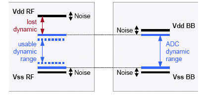
Figure 3 – Dynamic range reduction with analog interface
Finally, this interface introduces a lot of trouble for the designers of the BB chip. This chip may be a large SoC containing a small area reserved for the WLAN functionality. The requirement for high performance fast A/D and D/A converters in such - chips introduces constraints on the technology choice that may not be acceptable at all. The only solution in that case is to introduce a third chip in the system (WLAN BB) between the SoC and the WLAN RF. This goes against the general trend of integration and reduction of the components count.
The HiSS interface solution
Trade-off choices
After reviewing all the challenges brought in by the analog interface, a fully digital solution looks like the way to go. As highlighted in the introduction, as there are several BB designs for a single RF chip, it is worth putting more effort in the design of the latter if the integration of the WLAN functionality is easier afterwards. This line of reasoning is driven by NewLogic’s focus on IP and reusability.
The fully digital interface solution can take many different formats and we reviewed different possibilities, in order to optimally trade-off the complexity, clock speed, data rate, number of pins and reusability of the interface. The global system cost issues (due to silicon and PCB area, number of pins, required components, PCB electrical characteristics…) were one of the driving constraints.
Description of the HiSS interface
The interface that was designed (the HiSS interface, presented in Figure 4) allows a complete control of the radio from the baseband with only 11 pins and a clock frequency of 240 MHz, and using standard LVDS pads [6]. The baseband chip only needs digital logic, as all mixed-signal blocks (including the PLL that generates the interface clock) have been moved to the RF chip.
The signals to the discrete components, previously driven directly from the BB chip, now are outputs of the RF chip. Reducing further the pin count of the BB chip and the number of wires between the BB domain and the RF domain.

Figure 4 – HiSS interface
When switching from an analog interface to a fully digital interface, the A/D and D/A converters obviously have to be integrated into the RF chip. However, just doing this modification would require such a high data throughput requirement (of about 1 Gb/s) that it would either not be power efficient or would require too many parallel lines, thereby increasing the pin count and the system cost.
The idea behind the HiSS interface is to move to the RF chip the digital filters that process the data before the transmission and after the reception, as shown in Figure 5. The oversampling is therefore fully handled in the RF chip and the interface just has to sustain a more reasonable data throughput of 440 Mb/s. This is achieved with 2 parallel lines running at 240 MHz (total throughput of 480 Mb/s). This choice also allowed using standard LVDS (Low Voltage Differential Signaling) pads and does not draw too much current.
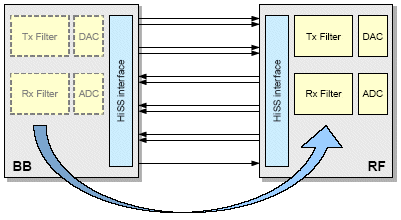
Figure 5 – New system split
Additionally, to further simplify the interactions between the BB and the RF chips, the packet detection and gain setting (AGC/CCA) procedure has been moved to the RF. This allows medium occupation monitoring without the need for the baseband to be active. This is very important to save power since a WLAN device spends most of its active time scanning for incoming packets. As the same interface is used to carry data samples and control information, a multiplexing scheme has been defined. This scheme translates in a simple protocol between the BB and RF chips, see Figure 6 and Figure 7 for control accesses, Figure 8 and Figure 9 for data accesses. This protocol requires hardware state machines to run on both sides, but the added gate count for the HiSS interface is very limited: around 3 kGates on each side.

Figure 6 – Register write access on the HiSS interface
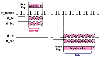
Figure 7 – Register read access on the HiSS interface

Figure 8 – Data transmission on the HiSS interface

Figure 9 – Data reception on the HiSS interface
Challenges of the fully digital solution
One of the challenges of the fully digital approach is that the architecture of the RF chip needs to be adapted. Indeed, the HiSS interface requires that the Tx and Rx filters be moved from the BB to the RF chip. This modification is not obvious and introduces significant complexity (several mm2 of digital gates) in the RF chip design. Moreover, adding so many gates in the RF chip reduces the options for technology choice and practically requires usage of CMOS technology.
Another inconvenience is the requirement for I/Os that can drive or receive low-voltage differential signals (LVDS). This signaling format ensures that the power consumption and electromagnetic noise are kept minimal. Though these I/O pads are present in mainstream technology libraries, they may not be available in some unusual processes and may need to be designed for implementation of the HiSS interface. However, this development is by far less critical than the design of high speed, high precision A/D and D/A converters.
Finally, the inclusion of about 1 kGates running at 240 MHz on a BB chip may be challenging depending on the design context. However backend tools and methodologies are now adapted to this kind of constraints and it is achievable within a reasonable time frame.
Benefits of the fully digital solution
Naturally the main reasons to move to a digital interface are primary benefits of the HiSS solution: the pin count is reduced, the baseband design is simplified and the BB chip becomes technology independent. However, other interesting qualities appear and bring a significant advantage over the legacy analog solutions.
As can be seen from the comparison between Figure 2 and Figure 4, the HiSS interface uses fewer pins than the analog interface. At best, a minimal analog interface would use 12 pins (Tx/Rx I/Q pairs, clock, 3-wire), a typical analog interface would use around 17 pins and some can go beyond 20 pins. The HiSS interface only uses 11 pins. This pin count reduction translates into a cost reduction, since the package cost is proportional to the number of pins and is a major part of the chip price. Both BB and RF chips benefit from this economy. It also reduces the required size on the PCB, leading to a more integrated solution and further cost reductions.
Moreover, the current HiSS interface can be very easily upgraded in the future to further reduce the pin count: by doubling the HiSS clock frequency – i.e. using a 480 MHz clock – the I and Q lines can be multiplexed in time. The protocol change is very trivial and this enhancement allows saving two differential pairs: the HiSS interface would then only feature 7 pins (see Figure 10). Consequently, at the expense of a higher clock rate, the BB/RF interface can be implemented with only 7 pins without compromising the performance of the system. Further pin count reductions (e.g. with bidirectional lines) can even be envisaged in the future, thanks to the move to the digital signaling. This is absolutely impossible with an analog interface.

Figure 10 – Possible enhancement of the HiSS interface
The second major benefit of the HiSS interface is its suitability to the SoC world. NewLogic focuses on the IP business and its customers need to integrate the WLAN baseband logic along with many other functions on large SoCs. It is impossible to dictate a specific silicon process to the system integrators: the WLAN portion is just an additional interface and should not disturb the rest of the design. The HiSS interface has moved out of the BB chip all the blocks that are linked to a specific technology: the A/D and D/A converters of course, but also the PLL and oscillator that generate the WLAN system clocks.
Figure 11 shows typical schemes for the clock distribution with an analog interface. Due to the low clock frequency that is imposed on the interface by the analog signals’ susceptibility to noise, the BB chip always needs to feature a PLL. However, as seen on Figure 12, the HiSS interface completely eliminates the need for a PLL, which is then simply replaced by digital dividers. This clocking scheme can now completely be handled in a fully digital design flow. The 240 MHz clock frequency chosen for the HiSS clock allows easy generation of various system frequencies with no or very low jitter.
Being fully digital and technology independent, the BB chip can now be implemented with very advanced technologies (90 nm and below). Technology shrinks are also made possible with a simple RTL synthesis operation. This technology independence allows significant area and power consumption savings for the BB chip, which are key in the portable products where the WLAN functionality is often requested.
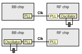
Figure 11 – Clock distribution with an analog interface

Figure 12 – Clock distribution with the HiSS interface
A long list of benefits now comes from the protection of the sensitive analog signals inside the RF chip, resulting from the move of the A/D and D/A converters. This offers an extremely good immunity to noise. The exposed interface is now digital, so the receptor of the HiSS data signals must only discriminate between two values, thus needs 6 dB of SNR, while an 8 bits ADC in an analog interface (best case) would need 50 dB of SNR. The matching problem on the PCB is also eliminated. Indeed it is easier to match the I and Q lines inside the RF chip than at the board level. The new system split also completely eliminates the dynamic range problem highlighted in Figure 3: the full range available in the RF can be used until the final conversion to digital. Moreover, as the RF chip is realized in a process that is better suited for analog (and RF), the performance of the converters is not compromised by design trade-offs.
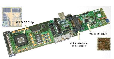
Finally, thanks to its robustness, the HiSS interface can carry signals over long distance (up to 1 m) and is well fit for e.g. laptop applications as highlighted earlier. The RF can now be very close to the antenna, reducing the length of the other sensitive part of the WLAN system: the RF signal link. The first HiSS-compatible system To prove our concept of interface, we have implemented the HiSS interface in a real IEEE 802.11a/b/g WLAN system (see pictures below). The RF and BB chips have been realized in TSMC 0.18 µm CMOS process, using the WLAN IP developed in NewLogic’s Sophia Antipolis R&D center.
It has been tested and validated, and the performance of the reception has been found to be better than competing commercial devices, in line with our simulations. No performance degradation has been detected due to the HiSS interface compared to a theoretical interface-less system composed of the same signal processing blocks. The versatility of the HiSS interface has also been demonstrated since the WiLD RF board has been plugged onto an FPGA board for validation purpose. The HiSS signals were driven by standard LVDS pads featured on the Xilinx FPGA used on the board. No single additional component was necessary to interface the digital part (inside the FPGA) to the RF chip.
Conclusion
We have seen that the analog interface exposes to the hostility of the outside world one of the most sensitive point in a WLAN system: the Rx analog signals. This is very dangerous and often ruins the efforts of the RF and BB chips designers to extract the best performance from their system. On the other hand, our fully digital BB/RF interface brings so many benefits that it has become the preferred system split choice of our customers when embedding WLAN baseband IP into their ASICs.
They experience savings in the development effort, by keeping the baseband part completely free of hard mixed-signal blocks and appreciate the increased robustness of the design. The HiSS interface will therefore probably have a bright future in embedded applications.
References
[1] “Wireless LAN Medium Access Control (MAC) and Physical Layer (PHY) specifications”, IEEE Standard 802.11 – ISO/IEC 8802-11:1999, March 18th, 1999
[2] “Wireless LAN Medium Access Control (MAC) and Physical Layer (PHY) specifications: High-speed Physical Layer in the 5 GHz Band”, IEEE Standard 802.11a, September 16th, 1999
[3] “Wireless LAN Medium Access Control (MAC) and Physical Layer (PHY) specifications: Higherspeed Physical Layer Extension in the 2.4 GHz Band”, IEEE Standard 802.11b, September 16th, 1999
[4] “Wireless LAN Medium Access Control (MAC) and Physical Layer (PHY) specifications: Further Higher Data Rate Extension in the 2.4 GHz Band”, IEEE Standard 802.11g, June 27th, 2003
[5] “RF-BB interface”, JEDEC Standard JC61, not yet published
[6] “Standard for Low-Voltage Differential Signals (LVDS) for Scalable Coherent Interface (SCI)”, IEEE Standard 1596.3-1996, March 21st, 1996
Related Semiconductor IP
- 8MHz / 40MHz Pierce Oscillator - X-FAB XT018-0.18µm
- UCIe RX Interface
- Very Low Latency BCH Codec
- 5G-NTN Modem IP for Satellite User Terminals
- 400G UDP/IP Hardware Protocol Stack
Related Articles
- Choosing serial interfaces for high speed ADCs in medical apps
- Integrating High Speed Serial Transceivers into an FPGA
- Multi-Gigabit SerDes: The Cornerstone of High Speed Serial Interconnects
- High Speed Serial Interconnects - What to Look for When Selecting an IP Vendor
Latest Articles
- SNAP-V: A RISC-V SoC with Configurable Neuromorphic Acceleration for Small-Scale Spiking Neural Networks
- An FPGA Implementation of Displacement Vector Search for Intra Pattern Copy in JPEG XS
- A Persistent-State Dataflow Accelerator for Memory-Bound Linear Attention Decode on FPGA
- VMXDOTP: A RISC-V Vector ISA Extension for Efficient Microscaling (MX) Format Acceleration
- PDF: PUF-based DNN Fingerprinting for Knowledge Distillation Traceability