Adding Hardware Acceleration to the HVL Testbench
By Author Yogesh Mittal, Freescale (yogesh dot mittal at freescale dot com)
ABSTRACT
Verification of an advanced automotive cluster chip is a complex activity because of multiple peripherals, high graphical processing requirements and software interaction for image processing.The verification effort needs to be augmented with the pre-silicon validation also to iron-out long simulation time related issues and the same platform also acts as demonstrable platform to customers. Consequently, such a complex system design requires modeling, verification, debug and analysis at different levels of abstraction with varying levels of precision. With higher complexity, the simulation times for system level verification increase multifold, and this has a big impact on turnaround time. Improving simulation time through hardware acceleration or in-circuit emulation are two approaches, but they would result in losing the benefits of a coverage-driven constrained random verification environment, as well as discarding the earlier setup for the hardware software co-verification. Thus, an integrated solution that provides acceleration, configurability and reuse is required. In this article, we describe how this can be achieved through the creation of a reusable transaction-level verification environment in HVL (System Verilog/System C/C++) for the system-level validation. This environment is capable of working at different levels of abstraction. It can also be heuristically and optimally partitioned between the hardware and software so that the complete environment can be simulated at significantly higher speeds while reusing the constrained random generation capabilities of the language.
1 Introduction
The verification of the complex design requires constraint driven random verification enabled testbenches to ensure full functional coverage and random scenarios. But the usage of high level of constraints causes higher simulation times for system level verification, and this has a big impact on overall design cycle time. This paper describes a framework where advance HVL based testbench can be reused to generate the hardware acceleration platform to overcome simulation speed bottleneck and save bring up time of such effort. The various schemes to maximize the performance of hardware acceleration solution are also mentioned in the paper.
2 Need for Reusable HVL Testbench and Hardware Acceleration
2.1 Device Feature Proofing and HW-SW Co-verification
It is imperative that feature feedback be elicited from the potential customer by providing an early demonstrable model of the device. This will ensure that a feature or critical functionality, that would otherwise not be discovered until the product was completed, is not missed out. The key challenges that make it difficult to meet a delivery date result from the misinterpretation of the hardware functionality specifications and the inability to efficiently integrate the software with the hardware. In a conventional flow, the platform for the software validation is not available until the device is available. The hardware/software co-verification usually involves just low-level software, consequently creating testbenches with behaviour that does not closely match the way actual software will run. The lack of testbench infrastructure reuse across teams is another issue
2.2 Equivalence Check between Functional Model and RTL
During device modeling, it is necessary to ensure that the RTL and the architecture model stay in sync and are functionally equivalent. Functional equivalence can be established and governed by creating a set of common tests that drive the functional model, as well as the RTL model. Hence, the architecture of the testbench should work with different abstraction level but without changing the underlying implementation or algorithm. With such a testbench, a golden test suite can then be defined to ensure the equivalence of the various models at different levels of abstraction during the SoC development cycle. A key challenge is to map the required scenarios in the form of cycle-based transactions to drive the architecture model has to functional signals to connect to the RTL world.
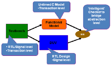
Figure 1: Equivalence check between Model and DUV
2.3 Inadequate Simulation Performance:
System-level validation of complex chips requires long simulation times, which becomes a big bottleneck Given the different characteristics of various parts of an SoC, orthogonal verification technologies (such as coverage instrumentation, assertions, PLI applications and debug) are needed to drive the verification process. The sheer size of these SoCs throttles the memory requirements of a verification platform. Simulation optimizations, efficient testbench design can only provide speedups only to a specific extent. Hence, there have been efforts to look at solutions beyond software simulators. Some of the approaches to accelerate the simulation speed include:
- In-circuit emulation: It requires a target board on which the entire design is mapped. However, there are structural differences between the actual netlist and the mapped netlist, and this may lead to masking of some critical design issues. It may also not be available early enough in the design cycle; moreover the available solutions are very expensive in nature.
- Synthesizable Testbench (STB) Approach: The design of such a testbench can be time consuming and can be difficult to debug. In addition, these testbenches cannot take advantage of advanced testbench techniques like constraint random verification and functional coverage.
3 Setting up the Transaction-based Acceleration Framework
3.1 Planning Simulation Acceleration approach
In order to speed up our simulations without compromising on debug features, we capitalize on the benefits of a transaction-based acceleration (TBA) regression environment. It enables advanced verification techniques to be applied while also allowing the reuse of most key simulation components. The TBA approach provides a significant level of performance improvement but requires careful planning and compliance with TBA methodology. The upfront development time is also relatively insignificant once this methodology is established. The basic concept of TBA is illustrated in the following figure.
In order to use TBA effectively, these two basic rules must be followed.
- Maximize overall performance by optimally partitioning between SW and HW
- Maximize simulation testbench reuse to save development time and resources
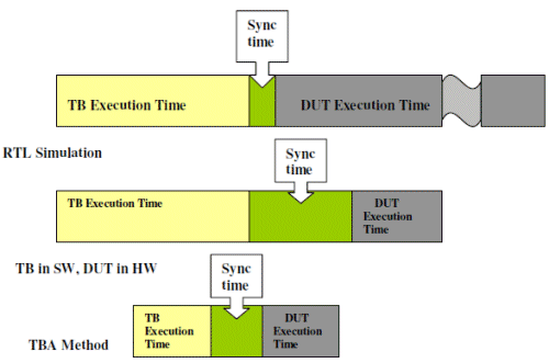
Figure 2: Simulation Acceleration Timing Profile
Therefore, messages between the simulated testbench and the synthesized testbench should be at the highest applicable level of abstraction. Maximizing the performance of the testbench by minimizing the time spent in the testbench would also offer the best results. The architecture should incorporate the following principles:
- The most active part of the testbench (BFM/monitors) should run in the hardware at actual speed.
- The testbench that resides on the SW side should be abstracted to higher-level data items or user transaction-level API to make it run significantly faster
- Testbench profiling should be done to improve the simulation performance.
- The BFMs/monitors are the only testbench components requiring clocks. When running on the accelerator, all clocks can be generated inside the HW side partition, avoiding synchronization with the SW side on every clock edge.
- BFMs/monitors can provide or gather “transaction data” over multiple clock cycles. During these periods the HW side can run without interruption.
- Transactions are stored in a buffer on the HW side and transactions are fetched only when the buffer level falls below a threshold to decouple SW and HW interactions on cycle by cycle basis.
3.2 Reusable Verification Environment
In order to reuse and extend the simulation environment to the hardware accelerator, it is imperative to use HVL like System verilog/System C/C++ to raise the level of abstraction. The objective is to create a ‘signal independent’ untimed transaction based environment in HVL first and then connect it to the low level drivers/BFM of simulation testbench or hardware accelerator. By creating such a layered testbench the high level stimulus/scenario remains consistent across simulation and hardware accelerator. In Figure 3 the reuse across simulation and hardware acceleration environment is shown as dotted line.
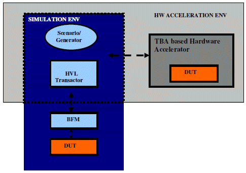
Figure 3: Reusing and extending simulation environment to hardware acceleration
3.3 Transactor Development
A Transactor is an interface that is used to establish a seamless communication between HVL
Testbench running on SW and the design running on the HW. It basically consists of two parts
- Front-end: C++ (SC/SV) model to send/receive high-level commands (transactions) to/from TB.
- Back-end: Synthesizable HDL BFM to convert high-level commands into bit-level protocol
Apart from above Transactor should be capable of controlling the start/stop of the clock to establish the synchronous relationship between SW and HW/
The TBA platform is composed of a software part on which the HVL test bench is run and a hardware part where the DUT is run along with other monitors/test components. The SW and HW communicate through ‘Messages’. On the software side, a C++ API allows messages to be sent and received to and from the HW. The HW part of the Transactor processes the messages and generates appropriate signals to stimulate the DUT.

Figure 4: HW-SW view of the Transactor
In this scheme only the transaction level arguments and return values across the HW-SW boundary, and all the higher bandwidth signal generation takes place on the HW side only. Following Figure demonstrates a memory transaction between the DUV and SW/testbench.
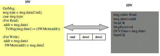
Figure 5: Example encapsulation of Transaction into Message
3.4 Connecting HVL Testbench to Hardware
A low cost ‘Client’ and ‘Server’ based methodology is used to connect the simulator running on the host machine to the DUT mapped on the hardware. The socket is opened to create a bridge across the two with DUT as the ‘Server’ and testbench as the ‘Client’. A socket is one end of an inter process communication channel, which the client and server use to communicate with each other. The client and server establish their own socket.
The socket interface eliminates the need for any third party tools and software (Figure 6). The software and hardware communicate through a ‘communication channel’ setup through a Physical layer e.g. USB. The Physical channel carries messages, as described earlier. The testcase in HVL side includes initialization of the sockets along with device configuration. After completing the initialization of the server component, the testbench waits for socket connections to be established by the client residing in the ’Server- Host’. Once the connection is established, the ‘server-host’ can initiate the transactions towards the device through the physical channel.
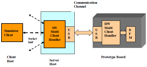
Figure 6: Integrated HW-Simulator Platform (USB is shown as an example)
3.5 Maximizing the Performance
3.5.1 Buffering Mechanism:
In order to minimize the HW-SW interactions on cycle by cycle basis, FIFOs are provisioned to store the stimulus before it is read out by the DUT clock/clocks. In case of reactive Transactor the communication between HW and SW need to be established before any further stimulus is applied. It can considerably slow down the simulation speed. The HW-SW interaction required in this case can be decoupled through these FIFOs. A programmable threshold is maintained in the FIFO and further transactions are fetched from the SW as soon as FIFO depth falls below the configured threshold. Similarly transactions are sent to the SW side when the FIFO goes above the configured threshold.
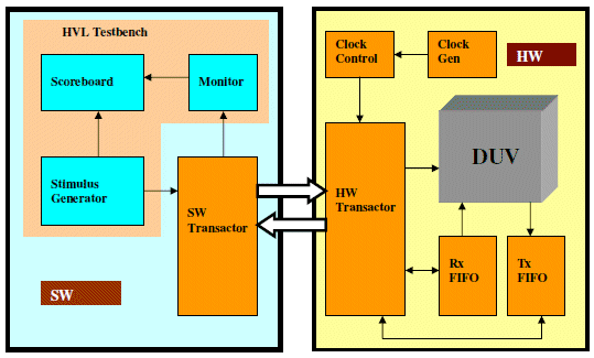
Figure 7: HW-SW partitioning
3.5.2 Clock control Mechanism:
As HVL testbench is running slower as compared to DUV ported in the hardware so a speed bridge is required to maintain the coherency between simulator and the actual DUV in the hardware. Each clocking interface of the DUV can be configured through “ClkAPIs” for the frequency, duty cycle, bus width of the data etc The simple scheme to decide the clock generation is based FIFO fill of the transmit buffer.
In case of multiple clocks, the clock edge generation process starts only when all transactors are ready. Also the fastest Transactor which runs out of data earlier halts other transactors by broadcasting the ‘StopClk’ message. The Figure 8 shows clock freeze, unfreeze during interaction between the HW-SW Transactors.
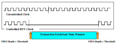
Figure 8: Clock Generation mechanism
4 Conclusions and Recommendations
The HVL layered Testbench based approach helped in building a well organized testbench structure, which can be reused from simulation to hardware acceleration. In this paper we presented a low cost TBA based acceleration scheme based on Client-Server communication and Transactor. The SW side of the Transactor is implemented as a sub-routine which is called by Testbench. The HW side of Transactor is implemented in HDL and then synthesized and mapped on the FPGA of platform. Several schemes were discussed to reduce the communication overhead between the SW and HW. We expect that proposed idea would be helpful in establishing a low cost simulation acceleration engine.
5 References
1. Synopsys VMM Hardware Abstraction Layer User Guide
3. SCEMI(Standard co-Emulation Modelling Interface) Reference Manual
4. Incisive Enterprise Palladium Series with Incisive XE Software datasheet
Disclaimer
We do not guarantee the accuracy or completeness of the information and nothing in this document shall be construed to be a presentation of such a guarantee. Any opinions expressed reflect the current judgment of the author of the relevant article or features, and do not necessarily reflect the opinion of Freescale Semiconductors. The opinions presented are subject to change without notice.
Related Semiconductor IP
- ReRAM NVM in DB HiTek 130nm BCD
- UFS 5.0 Host Controller IP
- PDM Receiver/PDM-to-PCM Converter
- Voltage and Temperature Sensor with integrated ADC - GlobalFoundries® 22FDX®
- 8MHz / 40MHz Pierce Oscillator - X-FAB XT018-0.18µm
Related Articles
- IP Core for RAID 6 Hardware Acceleration
- Hardware Acceleration of Kolmogorov-Arnold Network (KAN) in Large-Scale Systems
- SoCs: Supporting Socketization -> Developing a configurable testbench
- SystemVerilog 3.1 adds assertions and testbench automation
Latest Articles
- An FPGA-Based SoC Architecture with a RISC-V Controller for Energy-Efficient Temporal-Coding Spiking Neural Networks
- Enabling RISC-V Vector Code Generation in MLIR through Custom xDSL Lowerings
- A Scalable Open-Source QEC System with Sub-Microsecond Decoding-Feedback Latency
- SNAP-V: A RISC-V SoC with Configurable Neuromorphic Acceleration for Small-Scale Spiking Neural Networks
- An FPGA Implementation of Displacement Vector Search for Intra Pattern Copy in JPEG XS