H.264 Baseline Encoder with ADI Blackfin DSP and Hardware Accelerators
Mark Cox, Analog Devices Inc., Norwood, USA
Shankar Malladi, Analog Devices Inc., Norwood, USA
Issam Nsibi, Ebsys Technology, Tunis, Tunisia
Abstract
Numerous industries in broadcast, cab le, videoconferencing and consumer electronics space are considering H.264 as the video codec of choice for new products and services. The H.264/AVC video coding standard achieves a significant improvement in coding efficiency with increased computational complexity relative to former standards [2]. This creates a big challenge for efficient hardware and/or software implementations. In this paper, architecture and implementation of H.264/AVC baseline en coder for D1 resolution at 30fps using ADI Blackfin DSP and Hardware accelerators in FPGA is described. FPGA accelerators perform the processing required till generation of the Quantized coefficients (Loop1) for the Blackfin DSP to perform the entropy coding (Loop2). Bit rate control and quantization parameter (Qp) calculation is performed in the DSP while FPGA provides the frame level parameters to ADSP for acceleration of bit rate control, and calculation of Qp.
1. Introduction
The primary motivation to go for the H.264 encoder co-processor approach was the scalability in terms of meeting the processing power, cycle count, better control of logic implementation to accommodate late requirements changes, ease of enhancement to support HD resolution. Also, more significantly this implementation targeted to have more complex motion estimation, motion compensation blocks as part of hardware partition freeing up more valuable processing power of the DSP.
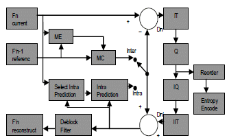
The Encoder operation has two major paths [2] as shown in Fig 1, the “forward” path consisting of motion estimation & compensation / intra prediction, calculation of difference, Integer transform, Quantization and Entropy coding. The “reconstruction” path is for generating refe rence frame which consists of Inverse Quantization, Inverse Transform, calculation of Sum (with the intra/inter predicted pixels) and de -blocking filter.

Figure 1. H.264 Encoder
2. Methodology for Hardware-Software Partitioning
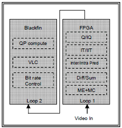
The hardware/software partitioning as shown in Fig.2 is arrived at based on profiling of computational requirements and data flow efficiency between software and hardware partitions. The computational requirements of various functional elements in H.264 encoder in the decreasing order are Motion estimation (ME), Deblocking filter (DF), Entropy coder, Inter/Intra prediction, Integer/Inverse integer transform (IT/IIT) and Quantization/Inverse Quantization (Q/IQ). The software partition running on Blackfin DSP (referred as “Loop2”) has Entropy coder (Motion Vector Prediction, VLC, Bit rate control) based on the DSP MIPS availability. The remaining encoder blocks in forward path (IT, Q, Motion estimation) and reconstruction path namely IIT, IQ, Intra Prediction, Inter Prediction and De - blocking filter are implemented as part of hardware partition (referred as “Loop1”) in the FPGA as accelerators. Motion estimation is developed as an IP core by ADI supporting resolutions from CIF to HD. Same IP is used as part of H.264 encoder implementation configured for D1 resolution.
Apart from the H.264 encoder blocks, other modules like input video capture (ITU.656 interface), DDR controller are also part of hardware blocks in the FPGA. In this hardware/software partitioning, the data flow direction is always from FPGA to DSP thereby enhancing the efficiency of DSP bus bandwidth utilization.
This architecture significantly eases the implementation in terms of DSP -FPGA interface, FPGA design for hardware blocks including complex modules like ME, inter/intra prediction, deblocking filter.

Figure 2 . Hardware/software partitioning for H.264 encoder
3. Design Details
Loop2 in Blackfin DSP and Loop1 in FPGA are running concurrently and they are pipelined at MB level.
FPGA takes in the video capture data from video decoder (for analog camera input) or directly from digital camera supporting ITU.656 standard. FPGA runs the forward and reconstruction paths on the captured frame. The output of forward path “Loop1” data (after ME, Diff, IT, Q) will be sent to the DSP as 1024 byte structure. Blackfin DSP runs the entropy encoding and bit rate control algorithm on the received structure data from FPGA and sends the H.264 encoded data to the network. This structure apart from quantized residual data contains the motion vectors and other parameters required for inter/intra prediction and deblocking filter. Two buffers are used in a ping pong manner to allow the pipelining between sending data to frame buffer and processing the next MB.
4. FPGA Implementation of Forward path modules
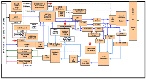
The detailed block diagram of the hardware accelerators in the FPGA co-processor is shown in the Fig.3.
Motion Estimation/Compensation Module (MEDMA)
The Motion Estimation DMA (MEDMA) IP engine from ADI provides an efficient, low-power means of performing high-quality motion estimation for video codec standards MPEG-4 and H.264 (MPEG-4 Advanced Video Codec, AVC) by using dedicated hardware to calculate motion vectors for each 16x16 macroblock in a frame. Motion Estimation is typically the most compute -intensive process in a video encoder and MEDMA acts like a simple DMA controller with programmable Rx and Tx channels to allow a software-based codec to easily integrate hardware acceleration into it’s flow. The hardware provides the following features and capabilities:
- Scales to a large range of frame resolutions and frame rates:
- QCIF (176x144) @ 15 frames per second requires a 2MHz input clock
- CIF (352x288) @ 30fps requires a 16MHz input clock
- D1 (720x480) @ 30 fps requires a 56MHz input clock
- HD 720p (1280x720) @ 30fps requires a 148MHz clock
- Integer pixel search window size of 80x48, with motion vectors generated to ¼-pixel precision
- Integer search algorithm provides close to Full Search performance
- H.264/AVC-compliant half- and quarter-pixel interpolation
- Full 8-point half- and quarter-pixel searches, +/- 0.5; horizontal, vertical and diagonal directions
- Rx and Tx DMA master channels with built-in automatic 2D addressing and frame boundary checking
- Reference window buffer data reuse performed in hardware to reduce DMA bus cycles
- Software bypass mode to allow use with other codec standards
- Interrupt-driven or semaphore-driven interface to software allows maximum flexibility for software control
- Four-stage search pipeline to maximize block utilization

Click to enlarge
Figure 3 FPGA Implementation of hardware accelerators
Data Fetch
This module fetches the current and reference window data for every macro block. This module interfaces with the DDR SDRAM controller in one side and the Intra SAD calculator, DIFF and MEDMA on the other side.
ME Control
The motion estimation (MEDMA) IP requires an on chip processor/ controller to program its internal registers both once a frame and once every macro block. It also writes out the motion vectors, minimum SADinter value and inter-predicted pixels (ME structure) to external memory. The ME control module reads and stores them in temporary buffers for encoder operation.
As the interface to MEDMA module is AHB, this module needs to implement a wrapper to take care of the AHB protocol. It implements a AHB Rx slave for receiving the ME structure and a AHB master to write into the registers of ME module.
Decision and Encoder control
This module takes the SADinter, SADintra, MVD, Qp (from ADSP registers) and generates the inter/intra bit, which is used by the DIFF and Curr MB Wr control module to read da ta from intra prediction buffer or inter prediction buffers for calculating the difference. This module also generates the sequencing control signals for all the other modules.
Intra SAD calculator
This module maintains pixels for top and left macro blocks (edges) of current frame, and performs a prediction (4x4 DC mode) every MB. After prediction is over, it takes the current MB data and calculates the “SADintra” value for the given macro block. This is value is used by the Decision module during “loop 1 encoder cycle”.
RD and 4x4 convert, DIFF & curr MB Wr cntrl
The data format of current frame is in pixel raster order. The encoder processing is performed on a 4x4 block within a macro block. Note that the current macro block data used by the ME module is in pixel raster within a macro block. This module converts the pixel raster data to a block raster format and feed for difference calculation. The DIFF and Curr MB Wr cntrl modules read the corresponding data from inter prediction buffers or intra prediction buffers based on inter/intra flag set by the Decision module. This module generates the read address from the current MB buffer (Fetch module) and for Buffers for Inter/Intra.
RD & Update cntrl
The “predicted pixels” (Inter luma/chroma, intra Luma/chroma) are stored in the Buffers and these are read by the DIFF module. After the sub block (4x4) difference data passes through the IT, Q, IQ, IIT phases, it is added with the corresponding “predicted pixels” for generating the sum output for deblocking filter. These sum outputs are also updated to the “Top and Left Pixels” buffer for intra prediction of subsequent 4x4 sub-blocks and Macro blocks. This sequencing is implemented by the RD & Update cntrl module which generates the read addresses for the buffer RAMs, and write addresses and Enable signals for the top and left pixels buffer.
Integer Transform (IT)
The integer transform (IT) gets data from a blockRAM interface with the DIFF sub -module. Each time 16 values are written, a ‘Ready’ pulse is generated to enable the 2-D transform.
The Integer transform block implements the following matrix multiplication

Where X is the input block for IT and Y is the output.
Quantization Parameter generator
The quantization and the inverse qu antization equations involve at least four parameters to be calculated and used - Qbits value, f_param, MV and V
Quantization (Q)
The Quantization (Q) consists of two operations: scaling and quantization. The scaling is a scalar multiplication of the transformed matrix with the following one:
QPluma and QPchroma values are read from interface registers with DSP and following equation is implemented:

I = 0...3, j = 0...3
MF, f and qbits are calculated at MB level
The Quantization module also counts the number of ONE within the current 4x4 block, and generates a flag resetOnes which is communicated to the inverse transform module.
Hadamard Transform and Quantization
The DC coefficients of luma form one DC block.
The DC coefficient of chroma for CR and CB each form one 2x2 block.
The grouped DC block of luma is transformed as follows:

The grouped DC blocks of chroma are further transformed as follows

The obtained 2x2 blocks are quantized in the same manner described above except that we have to shift by (qbits +1) instead of qbits.
The quantization of both DC coeff luma and DC ceoff chroma is done on the same way as AC coeff, except that the parameters used are modified.
5. FPGA Implementation of Reconstructed path modules
Inverse Hadamard Transform
Before rescaling, the obtained matrix is transformed using the same Hadamard transformation (luma and chroma). Then the rescaling uses a V parameter previously calculated on quantization parameter generator.
Inverse Quantization (IQ)
The inverse Quantization of the AC coefficient for both luma and chroma are evaluated using the following formula:

where, Vij are obtained from the look up table stored within FPGA.
Inverse Integer Transform (IIT)
For the inverse transform, t he post scaling operation is merged with the quantization process. The coefficients are multiplied by 2 and after the transform, the values in the final matrix are divided by 4 to get the final result. Both luma and chroma transform operation is done on 4x4 sub -block of pixels.
The Inverse transform module implements the following matrix multiplication

Here, [B] matrix is the input block of data from the inverse Quantization module. The 4x4 matrix values are divided by 4 at the final stage, 32 added and the value is divided by 64. The cycle count for this module is 366 cycles per macro block
Intra Prediction module
The term intra prediction refers to the fact that the prediction is performed relative to information that is contained only within the current frame and not relative to any other frame in the video sequence. In other words, no temporal processing is performed outside of the current picture or fr ame. Spatial and spectral redundancies are used while encoding such frames.
The Intra prediction module generates the predicted pixels of one block at a time for both luma and chroma pixels which are sent to the sum module to be added with the Inverse transform output. There are 9 optional prediction modes of luminance pixel intra-prediction for 4x4 blocks and 4 modes for 16x16 macroblocks. For chrominance samples there are 4 intra prediction modes. All these prediction modes are supported in this implementation. Generation of predicted pixel is based on the mode information of the block which is fetched from the structure fetch module. Predicted pixels are generated one block at a time and are sent for summation with the output of Inverse transform. The cycle count for this module is 460 cycles per macro block
Luma prediction is carried out on 4x4 block with the mode of prediction, availability info extracted from “MB parameter” in the structure data. For pixel 0-15 of each block, “enable” is generated fo r “Sum” that updates the output FIFO. When generating left edge pixels they are stored in the “left pixel buffer” for next block prediction. Similarly bottom edge predicted pixels are stored in the “pixel line buffer”. If prediction mode is “16x16” then left and line buffers are updated for the last pixels in a macro block only for Block1/2/3 MB0 prediction
For chroma prediction for each macro block, 4 blocks of 16 pixels each are considered and other steps remain similar to luma prediction
Inter Prediction module:
In inter prediction, the inherent temporal, or time - based redundancies are exploited to realize higher compression ratios. In the encoder, previously encoded frames are used as reference frames and only the difference is coded. In the present encoder implementation single previous frame is used as reference frame.
The inter prediction for luma data is done within the ME IP. The IP provides the information regarding the motion vectors as part of the structure output.
For chroma prediction for each macro block, 4 blocks of 16 pixels each are considered. Other steps remain similar to luma prediction. In the reconstructed frame data, Cb and Cr values are packed and stored in the DDR SDRAM. Cb and Cr values are unpacked and used for the Prediction of chroma pixel values.
SUM module
This module takes in the data from inverse transform module and intra/inter prediction module. It then performs sum & clipping of these two input data. This module works on 4x4 block basis with each pixel out in one cycle. There is 3 cycle latency in this module in the existing implementation.
Deblocking filter module
The final stage in the reconstruction path is deblocking filter which removes blocking artifacts between blocks. This module consists of three sub - modules BS compute, Alpha-Beta compute and Filter core modules.
The BS compute module generates 32 boundary strength values for 32 block edges within an MB. This module gets the required parameters from the structure fetch module, and calculates the BS value for each left or top edge of 4x4 sub-block within a given MB. It returns three 32 bit registers containing the BS values.
The Alpha-Beta compute module gets the fetched data from the structure fetch module, and calculates the three potential values of Alpha, the three potential values of Beta and the nine values of TC0, for luma. It does the same calculations for chroma data also.
The filter module acquires data at the output of the SUM module, the BS compute module and the alpha beta module (modules providing boundary strength and alpha/beta values for right and top edges of each 4x4 block in a macroblock) , and smoothes the edge between two 4x4 blocks.
Data is fed continuously to the filter, and four pixels are processed at the same time. The filter starts once the whole MB from SUM is ready. Left filter (vertical edge) of one 32 bits word takes three clock cycles. Top filter (horizontal edge) takes four clock cycles. The cycle count for this module is 84 cycles per macro block.
Reference frame write module :
This module interfaces with the deblocking filter module for reconstructing the frame within the frame buffer (DDR SDRAM). For luma, this module reads data from two blockRAM interface and forms DDR bursts. For chroma, it converts data from 4x4 format into 2x2 format, packs it into CbCr component and forms DDR bursts. The cycle count for this module is 155 cycles per macro block write to frame buffer.
6. Pipelining
The encoder operation is divided into 4 major pipeline cycles to match the cycle count requirement per macro block. The four cycles are as given below
- Fetch Cycle (reference frame search window and current frame data fetch)
- Motion estimation cycle
- Encoder cycle (Availability Load, MVD calculation, Decision, Intra Luma/chroma or inter chroma Prediction, Diff/Sum, IT/IIT, Q/IQ, Hadamard)
- De-blocking filter cycle (filter and reference frame write)
The 0th macro block goes through the Deblocking filter cycle after four-macro block cycle time latency. Deblocking filter writes the reference data into the DDR SDRAM for MB number 0, at the same time Loop2 and Loop1 encoder operate on MB number 1, Motion estimation is carried out for MB number 2, and Reference window & current frame data is fetched for MB number 3.
7. Results and Conclusions
For this design, ADI Blackfin processor running at 500MHz is used as the host and Xilinx Virtex-4 LX160 FPGA along with DDR SDRAM is used as the co-processor running at 75MHz. The DSP - FPGA interface is through external Async hronous memory bus. The H.264 encoder accelerator in FPGA is running at 75MHz. The resource utilization for this accelerator implement ation in FPGA is approximately 51K 4 -input LUTs, 25K Flip-Flops and 71 BlockRAMs.
A reference design platform is built for the validation of H.264 D1 encoder with BF561 Blackfin DSP and Xilinx XC4VLX160 FPGA. The same platform is used for H.264 encoder validation. The platform also includes support for analog video In/Out, memory interfaces for DSP and FPGA, Ethernet controller interface for DSP. Th e present H.264 encoder solution is validated on this reference platform for full performance (25fps for PAL/30fps for NTSC).
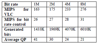
Theoretically, to achieve full performance of 30fps for NTSC or 25 fps for PAL, the encoder need to process one macroblock in 1850 cycles at 75MHz. The cycle-count required for implemented hardware accelerator in the FPGA is around 1800 per macro-block (sum of cycle count for each module). Of the 4 pipeline cycles, Encoder cycle is the critical path consuming upto 1800 cycles while other pipeline cycles are within the cycle count requirements. Following table shows the MIPS consumption for Loop2 in Blackfin DSP for entropy coding and bit rate control algorithm implementation. These numbers are provided for 1Mbps, 2Mbps, 4Mbps and 8Mbps bit rate encoding.

Table: Loop2 test results for DSP MIPS consumption
With this implementation, D1 frame enc oding is achieved with 30fps. This design can be scaled up to decode HD frames by appropriately boosting -up 75MHz speed of FPGA accelerators and operating frequency of DDR SDRAM interface.
Conclusion
Architecture and implementation of H.264/AVC baseline encoder for D1 resolution at 30fps using ADI Blackfin DSP and Hardware accelerators in FPGA is described. The reference platform has been tested for the functionality and performance. Also, the implementation is benchmarked with complex and popular test sequences
Acknowledgements
The authors thank Chiranjeev Acharya, Sriram N and Subramanian LS for their significant contribution in the successful implementati on and validation of H.264 D1 encoder.
References
[1] Anand V Kulkarni, Shankar Malladi , “H.264 Decoder with ADI Blackfin DSP and hardware accelerators”, IP’07.
[2] Iain E G Richardson, “H.264 / MPEG-4 Part 10 White Paper”, www.vcodex.com.
Related Semiconductor IP
- H.264 - Efficient video compression for high-quality streaming and playback
- H.264 Codec - Efficient video compression for high-quality streaming and playback
- H264 ENCODER IIP
- H264 DECODER IIP
- H.264 Audio & Video Decoder IP
Related White Papers
- H.264 Baseline Decoder With ADI Blackfin DSP and Hardware Accelerators
- Designing A Real-Time HDTV 1080p Baseline H.264/AVC Encoder Core
- MPEG-4 encoder on an embedded parallel DSP
- H.264 encoder design using Application Engine Synthesis
Latest White Papers
- ACE: Confidential Computing for Embedded RISC-V Systems
- Customizing a Large Language Model for VHDL Design of High-Performance Microprocessors
- CFET Beyond 3 nm: SRAM Reliability under Design-Time and Run-Time Variability
- Boosting RISC-V SoC performance for AI and ML applications
- e-GPU: An Open-Source and Configurable RISC-V Graphic Processing Unit for TinyAI Applications