H.264 Baseline Decoder With ADI Blackfin DSP and Hardware Accelerators
By Anand V Kulkarni, Wipro Technologies and Shankar Malladi, Analog Devices Inc.
Abstract
Numerous industries in broadcast, cable, videoconferencing and consumer electronics space are considering H.264 as the video codec of choice for new products and services. The H.264/AVC video coding standard achieves a significant improvement in coding efficiency with increased computational complexity relative to former standards [2]. This creates a big challenge for efficient hardware and/or software implementations. In this paper, architecture and implementation of H.264/AVC baseline decoder for D1 resolution at 30fps using ADI Blackfin DSP and Hardware accelerators in FPGA is described.
1. Introduction
There are many previous works with softwa rehardware implementation of H.264 decoder [1]. In this previous implementation motion compensation is implemented as the software block.
The primary motivation to go for the H.264 decoder co-processor approach was the scalability in terms of meeting the processing power, cycle count, better control of logic implementation to accommodate late requirements changes, ease of enhancement to support HD resolution. Also, more significantly this implementation targeted to have more complex motion compensation bl ock as part of hardware partition freeing up more valuable processing power of the DSP.
2. Methodology for Hardware-Software Partitioning
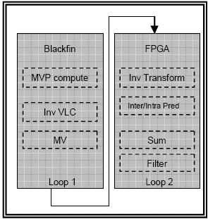
The hardware/software partitioning as shown in Fig.1 is arrived at based on profiling of computational requirements and data flow efficiency between software and hardware partitions. The computational requirements of various functional elements in H.264 decoder in the decreasing order are De-blocking filter, Entropy decoder, Inter/Intra prediction, Inverse transform and Inverse Quantization. The software partition running on Blackfin DSP (referred as “Loop1”) has Entropy decoder (Motion Vector Prediction, Inverse VLC) and Inverse Quantization based on the DSP MIPS availability. The remaining decoder blocks namely Inverse transform, Intra Prediction, Inter Prediction and De-blocking filter are hardware partition (referred as “Loop2”) in the FPGA as accelerators. In this hardware/software partitioning, the data flow direction is always from DSP and FPGA thereby enhancing the efficiency of DSP bus bandwidth utilization .
Also, the hardware-software partitioning allows the system to reorder the macroblocks in a sequential manner in cases where they arrive in a random order due to slice partitioning.
This architecture significantly eases the implementation in terms of DSP-FPGA interface, FPGA design for hardware blocks including complex modules like inter/intra prediction, deblocking filter.

Figure 1 . Hardware/software partitioning for H.264 decoder
3. Design Details
Loop1 in Blackfin DSP and Loop2 in FPGA are running concurrently and they are pipelined at frame level.
Blackfin DSP runs the entropy decoding and quantization on the received H.264 encoded bitstream from network and sends the entropy decoded, quantized data for every 16x16 Macroblock in the form 1200 byte structure to FPGA. This structure apart from quantized residual data contains the motion vectors and other parameters required for inter/intra prediction and deblocking filter. Two buffers are used in a ping pong manner to allow the pipelining between sending data to frame buffer and processing the next MB.
4. FPGA Implementation of Hardware accelerators
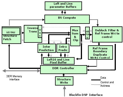
The detailed block diagram of the hardware accelerators in the FPGA co-processor is shown in the Fig.2.

Figure 2: FPGA Implementation of hardware accelerators
Structure Fetch module:
The “Structure Fetch” module fetches the structure data from frame buffer (DDR SDRAM memory) for Loop2 modules including inverse transform, intra prediction, inter prediction, de -blocking filter. To support fetching the data continuously it uses a dual port memory of size 128x128 (ping-pong). It can fetch and store the macro block of maximum size 64x128. This module takes 94 cycles to fetch structure for one macroblock.
The structure fetch module consists of an arbitration logic, control state machine, and structure RAM memory to store the structure data.
The Arbitration logic performs the following functions:
- Routing the requests from loop2 decoder modules Inverse, Inter-luma prediction, Inter-chroma prediction, Intra prediction and De-block filter to read the data from DDR SDRAM memory
- Prioritization of module requests and granting control of Buffer to the highest priority of module requesting the transaction.
The Control state machine takes care of
- Raising request to DDR SDRAM controller to fetch structure data
- Take care of ping pong structure data memory arrangement
Inverse Transform module:
For the inverse transform, t he post scaling operation is merged with the quantization process. The coefficients are multiplied by 2 and after transform, the values in the final matrix are divided by 4 to get the final result. Both luma and chroma transform operation is done on 4x4 sub-block of pixels.
The Inverse transform module implements the following matrix multiplication

Here, [B] matrix is the input block of data from the inverse Quantization module. The 4x4 matrix values are divided by 4 at the final stage, 32 added and the value is divided by 64. The cycle count for this module is 366 cycles per macro block
Intra Prediction module:
The term intra prediction refers to the fact that the prediction is performed relative to information that is contained only within the current frame and not relative to any other frame in the video sequence. In other words, no temporal processing is performed outside of the current picture or frame. Spatial and spectral redundancies are used while encoding such frames.
The Intra prediction module generates the predicted pixels of one block at a time for both luma and chroma pixels which are sent to the sum module to be added with the Inverse transform outpu t. There are 9 optional prediction modes of luminance pixel intra-prediction for 4x4 blocks and 4 modes for 16x16 macroblocks. For chrominance samples there are 4 intra prediction modes. All these prediction modes are supported in this implementation. Generation of predicted pixel is based on the mode information of the block which is fetched from the structure fetch module. Predicted pixels are generated one block at a time and are sent for summation with the output of Inverse transform. The cycle count for this module is 460 cycles per macro block
Luma prediction is carried out on 4x4 block with the mode of prediction, availability info extracted from “MB parameter” in the structure data. F or pixel 0-15 of each block, “enable” is generated for “Sum” that updates the output FIFO. When generating left edge pixels they are stored in the “left pixel buffer” for next block prediction. Similarly bottom edge predicted pixels are stored in the “pixel line buffer”. If prediction mode is “16x16” then left and line buffers are updated for the last pixels in a macro block only for Block1/2/3 MB0 prediction
For chroma prediction for each macro block, 4 blocks of 16 pixels each are considered and other steps remain similar to luma prediction
Inter Prediction module:
In inter prediction, the inherent temporal, or timebased redundancies are exploited to realize higher compression ratios. At the encoder, previously encoded frames are used as reference frames and only the difference is coded. In the present decoder implementation up-to 16 previous frames are used as reference frames.
The inter prediction module gets the reference frame number and motion vectors for each 4x4 block within a macro block from the structure data. These motion vectors are used to get 9x9 block data from reference frame data which is in the frame buffer. By using the 9x9 block data, inter prediction module calculates the predicted value of luma and chroma pixels and gives to the sum module. The cycle count for this module is 1300 cycles per macro block including reference frame data fetch cycles.
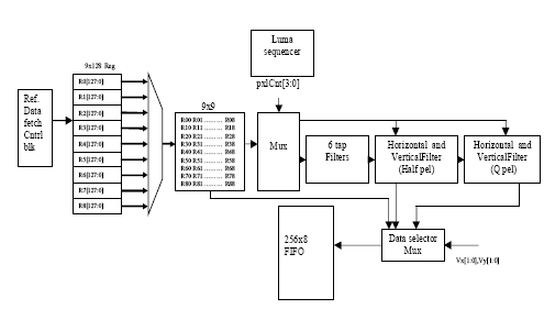
The block diagram of inter luma prediction block is shown in Fig.3. Inter Luma Prediction block consists of mainly two modules

Figure 3 Block diagram of Inter luma prediction block
a. Inter Fetch module: It gets the reference frame data from frame buffer and gives the 9x9 pixel window to the inter Prediction module
b. Inter Prediction module: It calculates the Luma and chroma pixel value according to the Vx, Vy value and for each macro block writes the pixels value to be sent to sum module. Full pixel, Half pixel and Quarter pixel precision is used for calculating predicted pixel values.
Predicted pixels are generated one block at a time and are sent for sum with the output of Inverse transform. According to Vx,Vy data of structure MB data the Half Pel, Quarter Pel calculations are made.
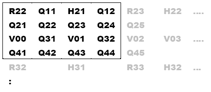
A pixel in a block can have one of the following values after inter prediction.

Based on the motion vector Vx and V y value, one of the 16 possible pixel values is written to output FIFO.
For chroma prediction for each macro block, 4 blocks of 16 pixels each are considered. Other steps remain similar to luma prediction. In the reconstructed frame data, Cb and Cr values are packed and stored in the DDR SDRAM. Cb and Cr values are unpacked and used for the Prediction of chroma pixel values.
SUM module:
This module takes in the data from inverse transform module and intra/inter prediction module. It then performs sum & clipping of these two input data. This module works on 4x4 block basis with each pixel out in one cycle. There is 3 cycle latency in this module in the existing implementation.
Deblocking filter module:
The final stage in the decoder is de -blocking filter which removes blocking artifacts between blocks. This module consists of three sub-modules BS compute, Alpha-Beta compute and Filter core modules.
The BS compute module generates 32 boundary strength values for 32 block edges within an MB. This module gets the required parameters from the structure fetch module, and calculates the BS value for each left or top edge of 4x4 sub-block within a given MB. It returns three 32 bit registers containing the BS values.
The Alpha-Beta compute module gets the fetched data from the structure fetch module, and calculates the three potential values of Alpha, the three potential values of Beta and the nine va lues of TC0, for luma. It does the same calculations for chroma data also.
The filter module acquires data at the output of the SUM module, the BS compute module and the alpha beta module (modules providing boundary strength and alpha/beta values for righ t and top edges of each 4x4 block in a macroblock) , and smoothes the edge between two 4x4 blocks.
Data is fed continuously to the filter, and four pixels are processed at the same time. The filter starts once the whole MB from SUM is ready . Left filter (vertical edge) of one 32 bits word takes three clock cycles. Top filter (horizontal edge) takes four clock cycles. The cycle count for this module is 84 cycles per macro block.
Reference frame write module :
This module interfaces with the deblocking filter module for reconstructing the frame within the frame buffer (DDR SDRAM). For luma, this module takes care of getting data from two blockRAM interface and forming DDR bursts. For chroma, it converts data from 4x4 format into 2x2 format, packs it into CbCr component and forms DDR bursts. The cycle count for this module is 155 cycles per macro block write to frame buffer.
5. Results and Conclusions
For this design, ADI Blackfin processor running at 500MHz is used as the host and Xilinx Virtex -4 LX80 FPGA along with DDR SDRAM is used as the co-processor running at 75MHz. The DSP - FPGA interface is through external Async memory bus. The H.264 decoder accelerator in FPGA is running at 75MHz. The resource utilization for this accelerator implementation in FPGA is approximately 21K 4-input LUTs, 13K Flip-Flops and 40 BlockRAMs.
A reference design platform is built for the validation of H.254 D1 decoder with BF561 Blackfin DSP and Xilinx XC4VX80 FPGA. The platform also includes support for analog video In/Out, memory interfaces for DSP and FPGA, Ethernet controller interface for DSP. This solution is validated on this reference platform for full performance (25fps for PAL/30fps for NTSC).
This implementation is benchmarked with complex and popularly known sequences such as “Football (American football, fast motion, camera motion) ”, “Mobile (Test sequence, high contrast, complex regular object motion, saturated colors, pan )” and “Stefan (Tennis player, high temporal activity, complex texture)”, which are encoded to 4Mbps streams. The DSP computing power needed for the said sequences are 366, 379 and 361 MIPS respectively.
Theoretically, to achieve full performance of 30fps for NTSC or 25 fps for PAL, the decoder need to process one macroblock in 1850 cycles at 75MHz. The cycle-count required for implemented hardware accelerator in the FPGA is around 1 600 per macro-block (sum of cycle count for each module). With this implementation, D1 frame decoding is achieved with 30fps. Though 4Mbps encoded streams are used for benchmarking, there is no such limitation in the FPGA implementation and it can handle higher bit rates as well. This design can be scaled -up to decode HD frames by appropriately boosting-up 75MHz speed of FPGA accelerators and DDR SDRAM interface.
Test Results: Loop1 and Loop2 benchmarking with popular test sequences.
| Test sequence | MIPS for Loop1 | Cycle count for Loop2 | Sequence characteristics |
| Football | 366 | 1400 | Fast motion, camera motion |
| Mobile | 379 | 1500 | High contrast, complex regular object motion, saturated colors, pan |
| Stefan | 361 | 1350 | High temporal activity, complex texture |
Conclusion
Architecture and implementation of H.264/AVC baseline decoder for D1 resolution at 30fps using ADI Blackfin DSP and Hardware accelerators in FPGA is described. The reference platform has been tested for the functionality and performance. Also, the implementation is benchmarked with complex and popular test sequences
Acknowledgements
The authors thank Chiranjeev Acharya, Wipro Technologies, India and Issam Nsibi, Ebsys Technology, Tunisia for their significant contribution in the successful implementation and validation of H.264 D1 decoder.
References
[1] Wagston Staehler & Altamiro Susin , “IP Core for an H.264 Decoder SoC”, IPSOC 2006.
[2] Iain E G Richardson, “H.264 / MPEG-4 Part 10 White Paper”, www.vcodex.com.
Related Semiconductor IP
- H.264 - Efficient video compression for high-quality streaming and playback
- H.264 Codec - Efficient video compression for high-quality streaming and playback
- H264 ENCODER IIP
- H264 DECODER IIP
- H.264 Audio & Video Decoder IP
Related White Papers
- H.264 Baseline Encoder with ADI Blackfin DSP and Hardware Accelerators
- The Hard Facts about Soft Interconnect IP
- How formal verification saves time in digital IP design
- High bandwidth memory (HBM) PHY IP verification
Latest White Papers
- ACE: Confidential Computing for Embedded RISC-V Systems
- Customizing a Large Language Model for VHDL Design of High-Performance Microprocessors
- CFET Beyond 3 nm: SRAM Reliability under Design-Time and Run-Time Variability
- Boosting RISC-V SoC performance for AI and ML applications
- e-GPU: An Open-Source and Configurable RISC-V Graphic Processing Unit for TinyAI Applications