Easy migration from Arm to RISC-V: an L110 case study
Laura Sartori, Codasip (February 14, 2025)
Last June, we launched the Codasip L110 RISC-V core, introducing the best-in-class solution for power-efficient applications. The L110 is highly competitive in terms of power efficiency and code density. Additionally, it is the first RISC-V core to support easy and risk-free customization while minimizing the verification effort required to bring these customizations to silicon.
Since then, we have been working with customers and partners who are interested in the new core for various reasons—whether as a RISC-V baseline for customization, a state machine replacement, or, most notably, as an Arm Cortex M0/M0+ class core replacement.
In this blog post, we will explore how Codasip L110 enables a seamless transition from Arm Cortex M0/M0+ cores—not only in terms of performance, power, and area (PPA) but also in system-level integration. This makes it easier for SoC hardware and software engineers to port between the two architectures.
More than one PPA point
Any backend engineer would tell you: there isn’t just one PPA number. PPA depends on numerous factors, including technology, frequency, features, and the target use case. Reporting PPA without specifying the running conditions can lead to misunderstandings and errors. This variability is even more relevant for the L110, as it is not a single core with fixed extensions and hardware features.
Thanks to its high level of configurability, we view the L110 as an IP family rather than a single IP. This flexibility allows our customers to, in collaboration with us, explore a broader PPA spectrum, optimizing for specific use cases. As shown in Table 1, we can gradually transition from a basic state machine replacement, the Aries configuration, to the Lyra configuration, which balances power efficiency, code density, and higher performance. Benchmark scores, such as CoreMark, significantly increase across different configurations, achieving much better CoreMark/MHz scores than Arm Cortex M0/M0+.
Each of these configurations can serve as an Arm Cortex M0/M0+ replacement, depending on your specific focus: area, code density, performance, or frequency. L110 provide fine-grained control over ratified extensions and hardware features, enabling precise PPA tuning.

Table 1: Examples of L110 configurations. The “Base Register” enables a very small core perfect for State Machine replacement. In yellow, extensions to increase the performance of the core. In purple, extensions which improve code density.
Memory system integration
The L110 has two separate memory buses: one for program instructions and one for data. In a Harvard system (image 1A), program and data are typically stored in separate physical memory regions. This separation prevents bus conflicts, enabling higher bandwidth and improved performance. This architectural advantage allows the L110 family to achieve CoreMark/MHz scores superior to that of M0 and M0+ and reaching that of cores such as the Arm Cortex-M3.
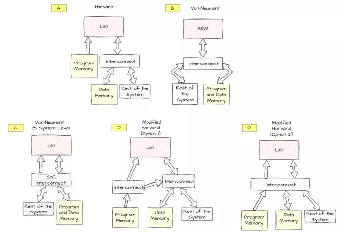
Image 1: L110 reference designs
In contrast, a Von Neumann architecture, used for M0 and M0+ (image 1B), uses a single shared bus for program and data access stored in the same physical memory. This shared bus can become a bottleneck, limiting the performance. On the other hand, a pure Harvard system requires special instructions and software to read data from the program memory.
There is a trade-off between performance and SW complexity mainly driven by your requirements and constraints.
You can interconnect L110 with any memory subsystem:
- Harvard (image 1A): Take advantage of the performance gain of two separated buses and physical memories.
- Von Neumann (image 1C): Replace Arm Cortex M0 and M0+ core with the L110. This aligns with what is expected from a Cortex-M0 and M0+ core and keep the SW support simpler. However there is a penalty in performance if compared to Harvard.
- Modified Harvard (image 1D, both options): Implement a hybrid system, where the core retains two buses and two memories but also allows access to program memory via the data bus. This provides a sweet spot between performance and SW complexity. Even though the program data is accessed through the data bus, avoiding the introduction of special instructions, the majority of the transactions will still occur in data memory, limiting the performance impact.
This is an example of how we offer different reference designs to match diverse customers’ system architectures, ensuring quick and efficient SoC integration validation.
Interrupt latency
A crucial aspect of Arm core replacement is ensuring short and deterministic interrupt latency.
The Core-Local Interrupt Controller (CLIC) is a proposed (yet to be fully ratified) RISC-V International standard, supporting both vectored interrupts and priority levels.
We have integrated CLIC into the core to support a configurable number of interrupts and priority levels. When incorporated into an SoC, the hardware integrator only needs to connect the required interrupts to other system components.
You can, at runtime, program a few of the CLIC features, such as the vectored interrupt lines, trigger type (level or edge), and polarity (0/falling or 1/rising edge), deferring the decision post silicon.
For vectored interrupts, the Interrupt Service Routine (ISR) is directly addressed via a vector table. This allows a fast identification of the interrupting device.
We have measured the L110 interrupt latency on a Genesys 2 FPGA platform. The minimal interrupt latency of L110 is 8 clock cycles in case of vectored interrupts and 6 clock cycles in case of non-vectored interrupts. We measured this as the latency from a valid interrupt until the first trap handler instruction is retired. We did not include the extra cycles which are required to identify the interrupt source in case of a non-vectored interrupt.
Depending on the register usage inside the trap handler, extra latency may be required to have them to the stack. In the worst case scenario this will be up to 31 clock cycles for RV32I and 15 for RV32E.
While closely following and implementing in HW the RISC-V CLIC standard, we have also ported the Nested Vectored Interrupt Controller (NVIC) API to our CLIC. This will facilitate an easy SW migration from Arm to RISC-V.
At Codasip, our hardware and software teams continue to collaborate with partners and customers to refine the best RISC-V processors. And, to ensure a seamless and efficient transition for engineering teams migrating from Arm architectures.
Are you ready to explore your options for migration from Arm to RISC-V?
Related Semiconductor IP
- 32 Bit - Embedded RISC-V Processor Core
- All-In-One RISC-V NPU
- ISO26262 ASIL-B/D Compliant 32-bit RISC-V Core
- RISC-V CPU IP
- Data Movement Engine - Best in class multi-core high-performance AI-enabled RISC-V Automotive CPU for ADAS, AVs and SDVs
Related White Papers
- CASE STUDY - Hands-on lessons from a legacy RT-level ATAPI IP Reuse
- An introduction to ARM Cortex-M0 DesignStart
- Case study: optimizing PPA with RISC-V custom extensions in TWS earbuds
- An FPGA-to-ASIC case study for refining smart meter design
Latest White Papers
- Breaking the Memory Bandwidth Boundary. GDDR7 IP Design Challenges & Solutions
- Automating NoC Design to Tackle Rising SoC Complexity
- Memory Prefetching Evaluation of Scientific Applications on a Modern HPC Arm-Based Processor
- Nine Compelling Reasons Why Menta eFPGA Is Essential for Achieving True Crypto Agility in Your ASIC or SoC
- CSR Management: Life Beyond Spreadsheets