Distorted Waveform Phenomena in 7nm Technology Node and its Impact on Signoff Timing Analysis
By Vismay Shah, Senior Physical Design Engineer and Dhruv Patel, Physical Design Engineer (eInfochips)
ABSTRACT
In today’s deep sub-micron technology nodes like 16nm, 7nm & beyond, there is a huge challenge for accurate static timing calculation. Ever increasing routing congestion, thin metal layers and moreover very high speed signal propagation make these nodes prone to significant crosstalk effects.
Aggressors can impact the slew of the victim signals resulting in waveform distortion, an effect that is also known as bumpy waveforms. At the 7nm node, the bumpy waveform effect causes major challenges for block closure. In this article, we will analyze the reasons for distorted waveforms and explore how we can overcome this effect as a physical design engineer.
In addition, we will discuss the root cause of the waveform distortion and its impact on signoff timing checks. This waveform majorly impacts the slew of the signal and it’s very difficult to accommodate such violations when the design is at the signoff stage.
These bumpy transitions are visible to physical design engineers only during timing signoff checks since PNR tools are not that accurate, compared to timing signoff tools. We will also show the practical impact on sign-off timing by applying two different methods of calculating delay.
Let’s dive right into it by looking at the challenges for timing accuracy.
Challenges for timing accuracy
Long tail effect
Scaling down effect has a tremendous impact on the thickness of the wires along with transistors. There is a significant increase in the resistance of the wires which results in increase in timing delay as well as the accuracy associated with timing models.
One of the critical parameters in measuring the timing of a cell accurately is a slew. Unfortunately, in lower geometry nodes, it is common to produce different waveforms because the device always takes finite switching time and its effect can no longer be avoided for accuracy purposes.
However, if we measure based on 10% and 90% measuring points, it’s not the accurate modelling with respect to a real world situation. An example is shown in the image below and the major difference in input waveform can be seen at the tail part which affects the output of the inverter so legacy measurement models for timing calculation is not good enough to parameterize the delay. The tail of the waveform has a significant impact in the computation of its delay.

Long tail effect (Image source: Cadence)
Back Miller cap
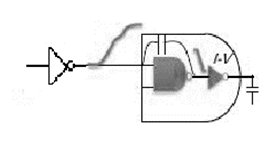
Back Miller cap (Image source: Cadence)
Miller Effect is the effective multiplication of the impedance across the negative gain of the amplifier. The Miller Effect arises in situations from a connecting capacitance across two nodes that have an inverting voltage gain/relationship between them. In the above example, consider first stage as an inverter and its outpin connected to AND (NAND+NOT) gate. Coupling capacitance of the internal nand gate (Cgd*gain) and first stage of receiver’s output can generate Back Miller cap. The next stage is an “aggressor”.
Traditionally, receiver pin capacitances are measured at slew thresholds, which are often 30% and 70% of VDD. As a result, the use of such thresholds in ECSM (Effective Current Source Model) libraries results in missing important data at the tail of the waveform. To capture above mentioned deep submicron effects like Miller Cap and long tail effects EDA vendors like Cadence recommend including 8-piece pin capacitances in ECSM library for accurate modeling.
The proposed extension of 3-piece capacitance tables to 8-piece tables allows better capture of the waveform distortions due to Back-Miller current at the waveform tail. The recommended 8-pc pin capacitance threshold values are 90% 70% 50% 40% 30% 20% 10% and 0.01% of VDD for fall transitions, and 10% 30% 50% 60% 70% 80% 90% and 99.99% of VDD for rise transitions.
What is Bumpy or Distorted waveform?
When the crosstalk-induced delay is analyzed, there is a potential for crosstalk to distort a victim switching waveform. A distorted waveform might deviate from the input waveforms used in the delay characterization of a receiving gate. This leads to inaccuracy in the slew-dependent delays in a downstream logic cone. If the crosstalk impact is severe, the victim waveform might become non-monotonic (bumpy) as shown in following diagram:
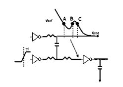
Bumpy waveform
In the above illustration, the victim net is coupled with coupling capacitance. The inverter (shown with the arrow) can cross its threshold three times from A to B to C. This can lead to inaccurate delay calculation if the proper model representation is not used.
In Cadence’s Tempus, one way to find out distorted waveform is by applying the below command. This can precisely tell what the aggressors are and how much it impacts on the overall timing delay. PNR tools are not able to see these SI (Signal Integrity) effects with the precision of timing sign-off tools, which causes a major challenge for the physical design engineer.
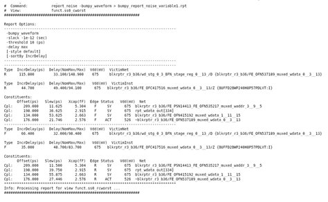
Download the PDF version to have a better quality image
Ways to analyze bumpy waveform for timing signoff
1. Non-linear (propagate bumpy to next level)

SI effects are significantly high in lower nodes below 22nm and need to be accommodated during the PNR stage. These effects from all the attackers can be modeled as current sources and, in turn, can be useful for creating input waveforms.
For nets with a high xcap, bumpy waveforms can be created with multiple transition crossings. Those bumpy waveforms are propagated to the next stage and can cause very large transition violations.
SI effects from all noise sources were combined through a non-linear simulation in the 1st iteration to create a final SI input waveform. For nets with large xcap, this simulation could result in waveforms with multiple transition crossings, or “bumps.”
Example 1:
As mentioned above, these distorted waveforms are propagated from 1st stage to 2nd stage. In case there are two back-to-back inverters connected as shown in below figure, there might be chances of the Back Miller-cap effect. This can amplify the violation and will be reported at the output pin of the 2nd stage of the inverter.

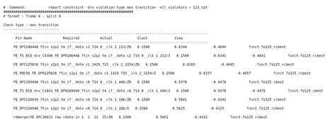
The below is an actual snapshot taken from block which is prone to the above situation where waveform distortion happens along with Back Miller cap effect where max transition slack is -484 ps:
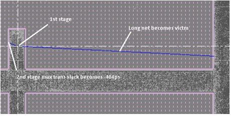
The following is a snapshot of Example 1, taken from Cadence’s Tempus tool. Whenever the tool propagates these distorted waveforms, it reports numerous max trans violations. This situation is certainly challenging during sign-off stage since these violations are not reported during PNR.
Download the PDF version to have a better quality image
2. Linear Method (convert bumpy to non-bumpy)
Propagating distorted waveforms to the 2nd stage complicates the delay calculation since it involves the next stage of combinational cells. The following method describes the way to model the non-bumpy waveform from distorted waveform.
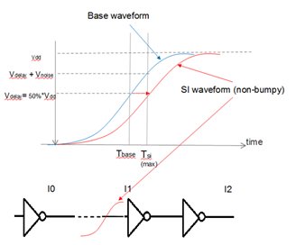
The tool will first calculate the total estimated noise peak as Vnoise through linear summation of noise source peaks and then stretch the base waveform by applying the total noise peak at the delay threshold Vdelay. The signoff tool calculates max delay crossing time Tsi as the time when base delay waveform crosses Vdelay + Vnoise For min, Tsi is the time when base delay waveform crosses Vdelay - Vnoise .
Use ratio = Tsi/Tbase to scale every time point on the base waveform so that the stretched SI waveform crosses the 50% VDD point at time Tsi. Then propagate the resulting stretched SI waveform through the cell.
There are no bumpy waveforms propagated to next stage, so expect to see fewer transition violations. In Tempus, one can enable the above method with specific commands.
In Tempus, by enabling the linear delay calculation mentioned above can significantly change the delay report even on the same net as shown in example 2. Now, the tool is reporting 31ps of slack for max trans.
Example 2:

Download the PDF version to have a better quality image
So, which method is preferable for timing signoff?
The above effects are more observable if the blocks have significant crosstalks. If we compare Examples 1 & 2, it’s clear that the linear method helps us to mitigate large timing violations, especially with regards to the large slew. However, the linear method can also vary timing calculation significantly even if the change in crosstalk is very small slew changes significantly as shown in the below image.

Image from Solvenet
The linear method can be accurate as long as the measurement of the slew is done at the most pessimistic points. However, in the following scenario when distorted waveforms are very close to the slew measurement trip points, this will result in change in overall path delay.
The hash marks along the waveforms indicate where the waveform is crossing the slew trip point threshold. For max-delay analysis, exact slew measurement uses the earliest crossing of the first slew trip point. Very slight changes in waveform shape can cause the waveform inflection to either reach or not reach the slew trip point, causing large changes in exact slew.
So, overall, both the methods have certain limitations; however, the linear method still gives a better picture in terms of the actual timing delay. At current juncture engineers are bound to face above challenges for block and design closure with regards to timing in 7nm technology.
References:
- https://solvnet.synopsys.com
- https://solvnet.synopsys.com/dow_retrieve/O-2018.09/dg/starolh/Default.htm#stug/about.htm?otSearchResultSrc=advSearch&otSearchResultNumber=2&otPageNum=1
- Static Timing Analysis for Nanometer Designs by J. Bhasker Rakesh Chadha, Rakesh Chadha, Springer Science-Business Media
- https://support.cadence.com/apex/HomePage
About the authors
Vismay Shah
Vismay Shah has been with eInfochips as a senior physical design engineer for over three years. He has more than 5 years of experience in the semiconductor industry. He holds a Master of Science degree from Arizona State University with specialization in mixed signal circuit design.
Dhruv Patel
Dhruv Patel is working as a physical design engineer at eInfochips. He has more than two years of experience in the semiconductor industry. He has holds a B. Tech degree from Nirma University in India.
Related Semiconductor IP
- NPU IP Core for Mobile
- NPU IP Core for Edge
- Specialized Video Processing NPU IP
- HYPERBUS™ Memory Controller
- AV1 Video Encoder IP
Related White Papers
- Cell model creation for statistical timing analysis
- Practical Applications of Statistical Static Timing Analysis
- Reducing Turnaround Time with Hierarchical Timing Analysis
- Removing pessimism and optimism in timing analysis
Latest White Papers
- Ramping Up Open-Source RISC-V Cores: Assessing the Energy Efficiency of Superscalar, Out-of-Order Execution
- Transition Fixes in 3nm Multi-Voltage SoC Design
- CXL Topology-Aware and Expander-Driven Prefetching: Unlocking SSD Performance
- Breaking the Memory Bandwidth Boundary. GDDR7 IP Design Challenges & Solutions
- Automating NoC Design to Tackle Rising SoC Complexity