Diamond Standard Processor Core Family Architecture
Introduction
Tensilica’s Diamond Standard Series is a family of 32-bit microprocessor and DSP Intellectual Property (IP) cores based on Tensilica’s Xtensa® Instruction Set Architecture (ISA). The base Xtensa ISA 24-bit instructions are targeted to a wide range of embedded applications. Most common instructions have a 16-bit narrow encoding as well, and the Diamond Series architecture allows modeless switching between 16/24-bit instructions. Consequentially, the Diamond Series processors achieve one of the highest code densities among all 32-bit RISC processors.
Some of the Diamond Standard processors, including the 545CK DSP, the 570T high-performance CPU and the 330HiFi audio processor utilize Tensilica’s innovative FLIX™ (Flexible Length Instruction eXtensions) technology for selective additional VLIW-style 64-bit instructions. The FLIX technology allows the issue of multiple operations per instruction, modelessly mixed with the native 16/24-bit instructions to increase the processor’s parallel-execution abilities and further boosts application performance.
This white paper explores the design of the Xtensa base instruction set architecture (ISA) and illustrates the impact of architecture on performance. It traces the evolution of modern instruction-set design and compares key features of Tensilica’s architecture with previous instruction set architectures. It provides a detailed rationale for the major architectural innovations in the Xtensa ISA.
The first section of this white paper gives a quick overview of the Diamond Standard family. The second section outlines the goals, philosophy and innovations inherent in the Xtensa instruction set. The third section gives a more detailed description, with a block diagram, of each Diamond Standard processor. Finally, the last section gives more information on strength of the Xtensa-based Diamond architecture, taking a look at benchmarks.
Diamond Standard Family Overview
Introduction
Tensilica’s Diamond Standard processor core family consists of two general-purpose controllers, a Linux-compatible CPU, a high-end 2/3-issue CPU, a high-performance audio processor, and a high-end DSP. All are ideal for SOC designers who require the absolute fastest time to market.
| Controllers | 108Mini | Ultra-low power, cacheless controller with rich interrupt architecture, minimal gate count for lowest silicon cost |
| 212GP | Flexible mid-range controller with instruction and data caches and user-defined local memory sizes | |
| CPUs | 232L | Flexible mid-range CPU with a Memory-Management Unit (MMU) for Linux OS support |
| 570T | Extremely high-performance, 2- or 3-issue static superscalar processor | |
| Audio | 330HiFi | Dual-issue static superscalar audio engine optimized for multi-format digital audio codecs (MP3, AC3, AAC, WMA, etc.) |
| DSP | 545CK | 3-issue VLIW, 8-way SIMD DSP |
The controllers and CPUs are optimized control-plane processors that are industry leaders in area, power consumption, code density and application performance. The Diamond 108Mini enables SOC architects to quickly integrate an efficient CPU into their designs. It is one of the smallest, lowest power 32-bit RISC controllers on the market, while achieving performance levels of much larger, complex CPUs.
The Diamond 212GP CPU is an area-wise and power-wise high-performance controller core with rich interrupt options and a single-cycle 16bit x 16bit MAC, which reduces the need to include a separate DSP in the system design. The Diamond 232L adds a MMU for Linux operating system support.
The Diamond 570T is a high-performance processor capable of issuing a 64-bit Very Long Instruction Word (VLIW) bundle consisting of two or three instruction slots. 64-bit multiple instruction bundles are created by the compiler if instructions can be issued simultaneously (the compiler may choose to create a bundle with a single instruction for performance reasons), otherwise a single 16/24-bit instruction is issued. The results is extremely minimal code expansion, due to ‘no-op padding,” as is the case with older fixed-length VLIW ISAs. Consequentially, the Diamond 570T code density remains high, at least 20% better than competing RISC architectures on industry standard benchmarks. The 64-bit bundles are freely intermixed by the compiler with 16/24-bit instructions, and the processor modelessly switches between 16-, 24- or 64-bit instructions.
The Diamond 545CK is a general-purpose DSP core. Like the 570T, the 545CK is capable of issuing 64-bit bundles with three instruction slots and modelessly switching between 16-, 24- and 64-bit instructions. Utilizing dual 128-bit load/store units, the 545CK DSP is capable of performing eight 16-bit MACs in a single cycle. This core is ideal for communications, audio, and imaging applications, employing a highly efficient and easy-to-program vector architecture utilizing Tensilica’s C/C++ compiler (XCC). The 545CK provides higher data throughput, lower power dissipation, and better DSP performance per watt and per area than any other DSP core. The 545CK offers, for the first time, a single core architecture that can be rapidly implemented to satisfy the specific requirements of any embedded application including control, protocol, signal, and image processing.
The Diamond 330HiFi Audio Engine also uses 64-bit bundles consisting of two instruction slots in addition to 16/24-bit instructions that are modelessly intermixed. The 330HiFi consists of a base Xtensa core with additional dedicated audio data registers and dual MACs that can operate on 24x24-bit or 32x16-bit data to achieve full 24-bit audio precision. Tensilica-defined instructions for audio codecs include load/store to auxiliary audio registers, bit-stream control, and specialized Huffman coding operations. Optional audio codec software for encoding and decoding most popular audio formats such as MP3, AC3, AAC, and WMA can be purchased separately from Tensilica. All audio codec software is pre-verified to execute efficiently on the Diamond 330HiFi processor.
Software Support
Software tools are provided with the Diamond Standard processors to ease system development. These tools consist of:
- A software tool suite to match the processor architecture. This tool suite includes XCC, a macro assembler, linker, debugger, and a basic software library. While XCC’s operation is similar to the GNU C and C++ compiler (GCC), XCC is an advanced optimizing compiler that provides superior execution performance. XCC also generates executable code with smaller code size relative to other compilers. XCC provides vectorizing DSP compiler support for the Diamond 545CK and bundles multiple operations into VLIW instructions for the multi-issue Diamond processors, the 570T, 330HiFi, and the 545CK.
- Xtensa Xplorer – Diamond Edition (DE), an integrated development environment based on the Eclipse platform. Xplorer DS serves as a cockpit for single- and multiple-processor SOC hardware and software design. Xplorer DS integrates software development and system analysis tools into one common visual design environment that provides powerful graphical visualization abilities and makes creating processor-based SOC hardware and software much easier.
- An instruction-set simulator (ISS) that is a cycle-accurate simulator for each of the Diamond processors. This pipeline-accurate ISS can be used for code benchmarking and enables faster code development, accurate performance modeling, and system-level architectural tradeoffs.
Feature Summary
All Diamond Standard processors share a common base of 16/24-bit instructions. Some Diamond processors add VLIW-style 64-bit instructions. Tensilica’s VLIW capability allows the issue of multiple operations per instructions, boosting the processor’s parallel execution abilities and application performance. Features include:
- Specialized functional units (not on all cores)
- Multipliers, 16-bit MAC, SIMD, VLIW
- Region-based memory protection, full MMU on Diamond 232L
- Miscellaneous processor attributes
- Big or little-Endian byte ordering (except 545CK, which is little-Endian only)
- 5-stage pipeline
- Exceptions: non-maskable interrupt (NMI), nine external interrupts, six interrupt priority levels, three 32-bit timer interrupts
- 32 entry (64 entry on 545CK) windowed register file
- Write buffer: 4/8/16 entries (depending on processor)
- Interfaces
- 32/64/128-bit Processor Interface (PIF) width to main system memory or to an on-chip system bus. Tensilica provides a complete Vera-based tool kit for PIF bridge implementation and verification.
- Inbound-PIF (e.g., DMA) requests allow external access to the processor’s local memory buses
- Ooptional AMBA AHB-Lite interface
- Direct I/O pins for the Diamond 108Mini, 212GP, and 570T processors
- Streaming data queues for the Diamond 570T, 330HiFi, and 545CK processors
- On-chip memory architecture (varies by processor, see figure 1)
- Programmable write-through or write-back cache-write policy
- Cache locking per line for set-associative cache
| Memory Type | 108Mini | 212GP | 232L | 570T | 330HiFi | 545CK |
| Local instruction RAM* | 1-128KByte | 0-128KByte | N/A | 0-128KByte | 0-128Kbyte | 1-128Kbyte |
| Local Data RAM 0 | 0-128Kbyte | 0-128KByte | N/A | 0-128Kbyte | 0-128Kbyte | 0-128KByte |
| Local Data Ram1 | 0-128Kbyte | N/A | N/A | N/A | 0-128Kbyte | 0-128Kbyte |
| Instruction Cache (set associativity) | N/A | 8KByte (2-way) | 16KByte (2-way) | 16KByte (2-way) | 8KByte (2-way) | N/A |
| Data Cache (set associativity) | N/A | 8KByte (2-way) | 16KByte (2-way) | 16KByte (2-way) | 8KByte (2-way) | N/A |
| Cache Line Size (I and D cache) | N/A | 32 bytes | 32 bytes | 32 bytes | 64 bytes | N/A |
* Processors with no instruction cache require at least 1KByte local instruction memory since vectors are mapped to local instruction memory due to performance reasons.
Figure 1 – Memory Architectures for Diamond Standard Processors.
- Processor development and debug capabilities
- C/C++ callable ISS
- On-Chip Debug (OCD) capability: Trace and instruction/data breakpoint support (two hardware-assisted instruction breakpoints and two hardware-assisted data breakpoints)
- GDB debugger support
- ISS and Co-Simulation Model (CSM) support for Mentor Graphics® Seamless™ Co-Verification Environment
- Robust EDA environment support
- Physical synthesis design flow
- Operating system support for Mentor Graphic’s Nucleus Plus, Express Logic’s ThreadX, Micrium Technologies’ μC/OS-II, MontaVista Software’s Linux Professional Edition, and Sophia Systems’ μITRON.
Code Density
The Xtensa ISA delivers highly efficient code that is as much as 50% smaller than today’s popular RISC and CISC architectures. The use of 24- and 16-bit instructions in the Diamond Series processors greatly reduces the size of application code compared to conventional 32-bit RISC code. Small code size helps to reduce on-chip memory requirements. The Xtensa ISA optimizes the size of the program instructions by minimizing both the static number of instructions (the instructions that constitute the application program) and the average number of bits per instruction. The use of 24- and
16-bit instruction words, the use of compound instructions, the richness of the comparison and bit-testing instructions, zero-overhead-loop instructions, register windowing, and the use of encoded immediate values all contribute to the Diamond Standard processors’ small code size.
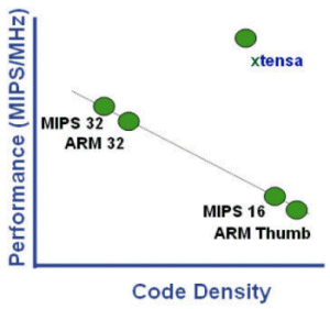
Figure 2. The Xtensa ISA Delivers Smaller Code and Better Performance.
The Diamond Standard processors also have several compound instructions that reduce the instruction count required to encode and execute a program. Compare-and-branch instructions, for example, constitute the most important class of compound instructions, reducing code size by at least 5%. Other compound instructions include shirt, add/subtract, and shift-and-mask.
The Diamond Standard processors (except the Diamond 108Mini) employ a feature common to DSPs but not on general-purpose architectures: zero-overhead loops – the ability to iterate a series of instructions without a branch at the end to loop back. With this feature, the Diamond processors can execute loops without stalls causes by branch mis-predictions or the need for extra instructions to decrement and test the loop counter. Reducing loop overhead improves performance and reduces code size.
The Diamond Standard processors employ register windows to reduce the number of instruction bits needed to specify a register. Because most instructions specify three registers (two source and one destination), register windowing results in substantial savings in code size. Register windows support a variable window increment size to allow call levels to completely fit into the Diamond processor’s 32-entry general-purpose
AR register file, thus minimizing the number of stack operations required to save and restore registers around call sites. The Diamond processors delay window overflow until absolutely necessary, creating fewer register-spill traps and smaller code size compared to other register-window architectures. It also means lower memory traffic and smaller code size than other non-register window architectures.
Principles of Instruction Set Design
The design of processor instruction sets is a well-established art. Most instruction set features are not new in themselves, but features can be combined in new and unique ways that advance the state of the art. In particular, when instruction set design is optimized for a different use than prior instruction sets, significant improvements result.
Instruction set architecture (ISA) design needs to balance many competing goals, including:
- The size of the machine code required to encode various algorithms
- The extensibility and adaptability of the ISA for new algorithms and applications
- The performance of processors that employ this ISA on such algorithms
- The power consumption of processors that employ this ISA on such algorithms
- The cost of processors that employ the ISA
- The ISA’s suitability for multiple future processor implementations
- The design complexity of processors that employ the ISA
- The ISA’s suitability as a target for compilation from high-level programming languages
The instruction set architecture has one direct and two indirect influences on processor performance. The ISA directly determines the number of instructions required to implement a given algorithm. Other components of processor performance include the minimum possible clock period and the average number of clocks per instruction. These are primarily attributes of the implementation of the instruction set, but instruction set features may affect the ability of the implementer to simultaneously meet time per clock and clocks per instruction goals. For example, a certain encoding choice might mandate additional logic in series with the rest of instruction execution, which an implementer would address either by increasing the time per clock, or by adding an additional pipeline stage, which will increase the number of clocks per instruction (instruction latency).
The RISC (Reduced Instruction Set Computing) processor design philosophy emerged in the 1980s. RISC ISAs allow implementers to reduce a processor’s cycles per instruction and clock period significantly without seriously increasing the number of instructions required to execute a program. RISC ISAs improve the performance of processors, lower design complexity, allow lower cost processor implementations at a given performance level, and are well suited to compilation from high-level programming languages.
Curiously, there is no single, completely comprehensive or satisfactory definition of the term RISC, but RISC processors typically include:
- Fixed-size instruction words
- 3-operand instruction orientation (two sources, one result)
- Large uniform register files for computation operations
- Simple and fixed instruction-field encoding
- Memory access via loads and stores of registers
- A small number (often 1, usually less than 4) of memory addressing modes
- Avoidance of features that would make pipelined execution of instructions difficult (variable latency and microcoded instructions).
On the other hand, most RISC ISAs – designed for high performance desktop computing environments where a large hard disk storage capacity is a given – are not optimized for producing compact machine code. In particular, RISC instruction sets usually require more program bits to encode an application than pre-RISC ISAs. In many embedded applications today, the cost of code storage (on-chip RAM / ROM) is often greater than the cost of the processor (gate count), so the use of RISC processors is sometimes limited in the most cost-sensitive applications.
An ISA that combines the advantages of RISC with reduced code size would be useful in many embedded applications. This combination is one of the underlying themes behind Tensilica’s development of the Xtensa ISA.
What Makes Xtensa Processors Unique?
The baseline Xtensa architecture builds on many of the principles of RISC, but introduces new techniques to improve both the number of instructions required to encode a program and the average number of bits per instruction. These techniques hold the promise to both improve performance and reduce cost relative to previous architectures. The Xtensa ISA starts with the premise that it must provide good code density in a fixed-length, high-performance encoding based on RISC principles, including a general register file and a load/store architecture. To achieve exemplary code density, Xtensa processors add a simple variable-length encoding scheme that doesn’t compromise performance. The Xtensa architecture further optimizes the cost of processor implementation by balancing such features as register files, control-flow operations, arithmetic and logic instructions and load/store capabilities in favor of operations that are frequent in modern embedded software and small and fast in modern deep-submicron implementation.
Registers
To maintain performance, a RISC instruction set must support at least two source register fields and one distinct destination register field. General register instruction sets that optimize only for code density are sometimes designed around two register fields – one used for source only and one used for both source and destination. This design approach sometimes reduces code size, but there is no way to compensate for the increase in the number of instructions required to execute a program. Instruction sets that specify fewer registers use narrower register fields and save bits per instruction. However, these instruction sets increase the number of instructions in the program by forcing more variable and temporary values to live in memory and they require extra load and store instructions.
Consequently, this design approach increases both the number of cycles for program execution and the power dissipated. As the number of the registers increases, the marginal benefits of a 2-operand instruction format decline. In particular, at least 16 general registers are required for good RISC performance. Three 4-bit register fields require at least 12 bits to encode. Bits for opcode and constant fields are also required. So 16-bit encoding, as used by some processors, is not sufficient for good performance.
The Diamond Standard processor cores employ a general purpose (AR) register file that contains 32 entries (64 in the Diamond 545CK). Instructions access this physical register file through a sliding 16-register window. Register windowing allows the Diamond processor to have a relatively large number of physical registers while restricting the number of bits needed to encode a source or destination operand address to four bits each. Thus the 3-operand instructions need only 12 bits to specify the registers holding the instruction’s three operands. This creates a compact, efficient instruction-encoding
scheme while maintaining the good execution performance that results from having a large available register file.
Register Windows
Register windows reduce code size and improve performance. Register windows are found on a few other processors, such as Sun’s SPARC ISA. The name “register window” describes the typical implementation where the register field in the instruction specifies a register in the current window into a larger register file. Register windows avoid the need to save and restore registers at procedure entry and exit. Instead of saving and restoring registers on a stack, a processor with register windows merely changes a register-offset pointer, which hides some registers from view and exposes new ones. The exposed registers usually do not contain valid data, and can be used directly. Register windows that overlap in their views of the physical register file between the caller and callee also avoid argument shuffling that can occur when arguments to procedures are passed in registers. Finally, register windows alter the breakeven point for allocating a variable or temporary to a register, and thus encourage register use, which is faster and smaller than using a memory location.
Unlike SPARC’s fixed-window overlap increment, the Xtensa ISA employs a variable increment for register windowing. This feature keeps implementation cost low by allowing a much smaller physical register file to be used. For example, many Sun SPARC ISA implementations use a physical register file of 136 entries, whereas Xtensa ISA implementations require a register file of only 64 entries to achieve similar performance. The Xtensa ISA specifies new methods to detect window overflow and underflow, and to organize the stack frame.
Instruction Width
Prior RISC architectures failed to achieve an appropriate balance between code size and performance because RISC ISA designers felt constrained to certain instruction sizes such as 16 and 32 bits. There are indeed advantages to using instruction sizes that are simple ratios to the data word width of the processor. However, relaxing the restriction somewhat has significant advantages that others have not explored. Xtensa processors use a 24-bit fixed-length encoding as a starting point; 24 bits are sufficient for achieving high performance while providing extensibility and room for powerful instructions that will decrease the number of instructions required to execute a program.
The Xtensa ISA’s 24-bit encoding represents a 25% reduction in instruction size relative to the more common RISC 32-bit instruction word, which reduces code size requirements relative to most 32-bit RISC instruction sets. Most importantly, 24 bits is simple to accommodate in a processor with 32-bit data-path widths.
The Xtensa architecture uses 4-bit register fields (see Figure 3), the minimum required for acceptable performance and the maximum that fits well within a 24-bit instruction word. Many RISC instruction sets use 32 registers (5-bit register fields). The difference in performance between 16 and 32 general registers (about 5%) is not as large as the difference between 8 and 16 general registers, and is small enough that other features can be introduced to make up the lost performance (e.g. compound instructions and register windows—see below). The resulting increase in the number of instructions needed to encode a program (also about 5%) is more than offset by the difference between 24-bit and 32-bit encoding (a reduction of 25%).
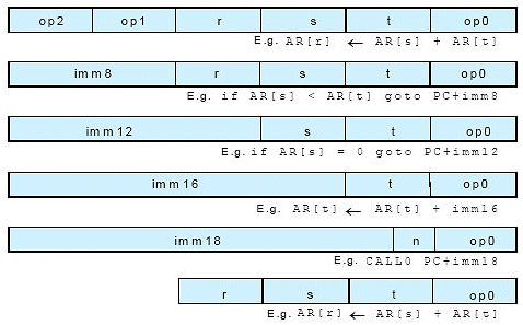
Figure 3: Xtensa Instruction Encoding Formats.
Note that many instruction sets with 5-bit register fields do not provide 32 general registers for compilation. Most dedicate a register to hold zero, even though the addition of a few extra instruction opcodes can easily eliminate the need for a zero register (e.g., the Xtensa NEG instruction). Also, other registers are often given specific uses that can be avoided by including other features in the instruction set. For example, the MIPS architecture dedicates two of its 31 general registers for exception handling and one more register for a global area pointer. So, in effect, the MIPS architecture provides the program with only 28 general registers for variables and temporary storage. That’s only 12 more registers than an instruction set that uses 4-bit register fields. The division of general registers into caller and callee saved registers by software convention is common and further restricts the utility of larger register files. The Xtensa ISA includes features that avoid this, which brings the effectiveness of the 16 registers almost to the level of other processors’ 32 registers. The Xtensa ISA shows that a 24-bit encoding of a full-featured RISC instruction set is possible. The Xtensa ISA is a significant step forward for processor design.
FLIX 64-bit Instructions
The Diamond Standard 570T, 330HiFi, and 545CK take advantage of Tensilica’s unique FLIX technology to schedule multiple operations in one 64-bit instruction. These wide-word instruction bundles allow more complex, compound machine instructions to improve code and application performance.
Unlike older fixed-length VLIW (Very Long Instruction Word) ISAs, the 64-bit-wide FLIX instructions are employed by the compiler when needed if instructions can be issued simultaneously (the compiler may choose to create a bundle with a single instruction for performance reasons), otherwise a single 16/24-bit instruction is issued. The results is extremely minimal code expansion, due to ‘no-op padding,” as is the case with older fixed-length VLSI ISAs. Consequentially, the code density remains high. The 64-bit bundles are freely intermixed by the compiler with 16/24-bit instructions, and the processor modelessly switches between 16-, 24- or 64-bit instructions.
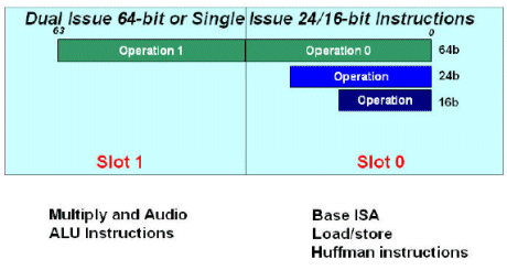
Figure 4. The Diamond 330HiFi uses Dual-Issue FLIX Instructions to Boost Performance.
Compound Instructions
To improve performance and code size, the Xtensa ISA also provides instructions that combine the functions of multiple instructions typically found in RISC and other processor instruction sets into a single instruction.
The first example of a compound instruction is a simple “left shift and add/subtract.” The high-end HP PA-RISC and DEC Alpha architectures are examples of instruction sets that provide these operations. Address arithmetic and multiplication by small constants often use these combinations, and providing these operations reduces the instruction count but potentially increases the processor clock period because of the additional series logic added to the computation pipeline stage. However, various implementations have shown that when the shift range is limited to 0 to 3, the extra logic is not the most critical constraint on the clock frequency. The ARM instruction set provides arbitrary shift and add and, consequently, many ARM ISA implementations have degraded maximum clock frequencies.
Right shifts are often used to extract a field from a larger word. For an unsigned field extract, two instructions (either left shift followed by right shift, or right shift followed by an AND with a constant) are typically used. Xtensa provides a single compound instruction, EXTUI (extract unsigned immediate), to perform this function. The EXTUI instruction is implemented as a shift followed by an AND with a specified mask that is encoded in the instruction word using just 4 bits. The logical AND portion of the EXTUI instruction is so trivial that its inclusion in the ISA is not likely to increase the clock period of Xtensa processor implementations. The same would not be true of an instruction to extract signed fields so there’s no corresponding EXTSI instruction included in the Xtensa ISA.
Branches
Most processor instruction sets, both RISC and otherwise (e.g. ARM, DEC PDP11, DEC VAX, Intel x86, Motorola 68000, Sun SPARC, Motorola 88000) use a compare instruction that sets condition code(s), followed by a conditional branch instruction that tests the condition code(s) for program flow control. Conditional branches constitute 10-20% of the instructions in most RISC instruction sets, and each is usually paired with a compare instruction. This style of instruction set is wasteful. Some instruction sets (e.g. CDC 6600, Cray-1, MIPS, DEC Alpha, HP PA-RISC, Sun SPARC V9) provide a compound compare and branch facility of varying flexibility.
The Xtensa ISA provides the most useful compound compare-and-branch instructions. Choosing the exact set requires balancing the utility of each compare and branch with the opcode space that it consumes, especially when 24-bit (as opposed to 32-bit) instruction encoding is the target. Other instruction sets fail this test. Compound compare-and-branch instructions reduce instruction count, when compared with instruction sets that have separate compare-and-branch instructions, and even when compared with the partial compare-and-branch instructions in the MIPS and DEC Alpha ISAs. Some Xtensa processor implementations may require an increase in clocks per instruction to implement some compound compare-and-branch instructions, but the overall performance effect of these compound instructions is still positive.
The Xtensa ISA’s compare-and-branch instructions also support comparisons to immediate values and use clever encoding of constants to increase their utilization. The BEQI, BNEI, BLTI, BGEI instructions also use a 4-bit field that encodes various common constants. The BLTUI and BGEUI instructions use a different encoding, as unsigned comparisons have a different set of useful values
The Xtensa processor’s compound compare-and-branch instruction sets pack all of these immediate values into a single instruction word, resulting in smaller fields. These instructions combine the comparison opcode, two source-register fields, and an 8-bit PC-relative offset target specifier into a 24-bit instruction word. The 8-bit relative target specifier will be too small in some infrequent cases so the compiler or assembler compensates by using a conditional branch of the opposite nature around an unconditional branch with a longer range. The Xtensa ISA also provides a series of compound compare-and-branch instructions that test against zero, the most common case. These compound compare-and-branch instructions have a 12-bit PC-relative offset, which provides much greater range.
The Xtensa architecture adds another important and unique goal to instruction set design: complete support for extensibility that allows for the addition of new data types, implemented in new instructions and closely coupled coprocessors. The Xtensa ISA uses an additional method for allowing coprocessor conditional branches. The Xtensa ISA offers an option that adds 16 1-bit Boolean registers. The Xtensa ISA’s BF (branch if false) and BT (branch if true) instructions test these Boolean registers and branch accordingly.
Xtensa ISA instructions can set the Boolean registers based on comparisons of their supported data types. All Xtensa processors share the baseline ISA’s Boolean register set and the BF and BT instructions. This approach makes efficient use of the Xtensa ISA’s short, 24-bit instruction word. This scheme is a new variant of compare-and-branch condition codes found in many earlier processor ISAs. The use of single-bit (Xtensa, MIPS) instead of multi-bit comparison-result registers (most other ISAs) increases the number of comparison opcodes required but decreases the number of branch opcodes required. This ISA design approach also makes the introduction of a broad range of application-specific branches and conditional operations simple and efficient for users to implement—a very important feature for an ISA designed expressly for extensibility.
The Xtensa ISA also provides a general-purpose, zero-overhead loop feature similar to that found in some DSPs (digital signal processors). Most RISC processors use their existing conditional branch instructions to implement software loops. However, this opcode economy increases program cycle count and consequently reduces execution speed. For many RISC ISAs, loop overhead consists of three instructions: add, compare, and conditional branch. The performance impact of the loop overhead is higher when the loop body is small. For small software loops, many compilers use an optimization called loop-unrolling to spread the loop overhead over two or more loop iterations, but this approach duplicates the loop body and significantly increases code size.
By contrast, many DSPs and some general-purpose processors provide other ways to perform certain kinds of loops. The first method is to provide an instruction that repeats the succeeding instruction a fixed number of times (e.g. TI TMS320C2x, Intel x86). For 1-instruction loops, a repeat prefix instruction eliminates loop overhead and saves power by eliminating the need to repeatedly fetch the same instruction within the loop. Some ISAs with repeat instructions require that the processor not take an interrupt during the loop. This limitation can impose unacceptable interrupt latency because loop execution may require many machine cycles to complete. An improvement on simple repeat prefix instructions is the ability to iterate a block of instructions multiple times with reduced or zero loop overhead (e.g. TI TMS320C5x).
The Xtensa ISA provides this zero-overhead loop capability via its LOOP, LOOPGTZ, and LOOPNEZ instructions in all Diamond Standard processors except the Diamond 108Mini. The Xtensa ISA’s LOOP instructions eliminate instruction execution cycles required for incrementing the loop index, for comparison and branch operations, and it avoids the taken-branch penalty that is typically associated with a compilation of loops based on conditional-branch instructions. The Xtensa ISA demonstrates how a reduced overhead looping capability can be integrated into a general-purpose processor ISA (as opposed to a DSP) to improve both execution performance and code size.
Overall, the Xtensa architecture makes six important contributions to general branch instructions:
- A choice of compare-and-branch instructions in a RISC ISA with the most useful comparisons
- Compare-and-branch with encoded immediate values, including branch-on-bit instructions
- Instruction formats with longer target specifiers for common cases (test against zero)
- The encoding of all branch instructions in a 24-bit instruction word
- Support for branches on coprocessor Boolean registers (condition codes) with logical operations on Booleans
- Zero-overhead loops that eliminate branch execution delay and reduce code size.
Limited Instruction Constant Width
No Xtensa baseline instruction is longer than 24 bits, so constant fields in the instruction word are constrained. The Xtensa architecture addresses this issue in several ways. The Xtensa ISA provides small constant fields to capture the most common constants. Xtensa instructions encode the constant value rather than specifying it directly. The encoded values are chosen from a wide array of program statistics as the N (e.g. 16) most frequent constants for each instruction type. The Xtensa architecture uses this technique in the ADDI4 instruction, where the 16 values are chosen to be -1 and 1 to 15, rather than 0 to 15. Adding 0 is of no utility (there is a separate MOVE instruction), and adding –1 is common. The constants used in bitwise-logical operations (e.g. AND, OR, XOR, etc.) represent bit masks of various sorts, and often do not fit in small constant fields. Bit patterns consisting of a sequence of 0s followed by a sequence of 1s, and a sequence of 1s followed by a sequence of 0s are quite common. For this reason, the Xtensa architecture has instructions that avoid the need for putting a mask directly into the instruction word. The EXTUI instruction (described above) performs a shift followed by a mask consisting of a series of 0s followed by a series of 1s, where the number of 1s is a constant field in the instruction.
Xtensa load and store instructions use an instruction format with an 8-bit constant offset that is added to a base address from a register. The Xtensa ISA both makes the most of these 8 bits and provides a simple extension method when 8 bits is insufficient. Xtensa load/store offsets are zero-extended rather than sign-extended because the values 128 to 255 are more commonly used by load and store instructions than the values -128 to -1. Also, the offset is shifted left appropriately for the reference size because most references are to aligned addresses from an aligned base register. The offset for 32-bit loads and stores is shifted by 2 bits; the offset for 16-bit loads and stores is shifted by 1 bit; and the offset for 8-bit loads and stores is not shifted. Most loads and stores are 32-bit, and so this technique provides 2 additional bits of range. When the 8-bit constant offset specified in a load/store instruction (or an ADDI instruction) is insufficient, the Xtensa ISA provides the ADDMI instruction, which adds its 8-bit constant shifted left by 8 bits. Thus a two-instruction sequence has 16 bits of range, 8 bits from the ADDMI, and 8 bits from the load/store or ADDI instruction.
Short Instruction Format
The Xtensa ISA consists of a core set of instructions that must be present in all implementations of the instruction set, and a set of optional instruction packages that may or may not be present in a given implementation. One of the most popular packages is the short instruction format package. It provides even further code size reductions by reducing the average number of bits per instruction. When these short-format instructions are present, the Xtensa ISA changes from a fixed-length (24-bit) instruction set to one with two instruction sizes (24-bit and 16-bit). Note that the Xtensa architecture does not employ modes to add the 16-bit instructions to the ISA the way some other RISC processors do. The Xtensa ISA’s 24- and 16-bit instruction formats are operative simultaneously so there is zero overhead incurred in switching from one instruction format to another.
Because the Xtensa short instruction forms are optional, these forms are used solely for improving code size; no new capabilities are added by the Xtensa ISA’s 16-bit instructions. The set of instructions that can be encoded in 16 bits consists of the most statically frequent instructions that will fit. The most frequently used instructions in most instruction sets are loads, stores, branches, adds, and moves; these are exactly the instructions present in the Xtensa ISA’s 16-bit instruction set.
Only the most frequent instructions need short encodings, so three register fields are still available (because the opcode field is small) and narrow, encoded constant fields can capture a significant fraction of the uses. Approximately half of the Xtensa instructions needed to represent an application can be encoded in just six of the sixteen opcodes available in a 16-bit instruction encoding after three 4-bit fields are reserved for register-specifiers or constants.
External Processor Interface (PIF)
The PIF connects the core to any proprietary or standard system bus. The PIF width depends on the specific Diamond core (32 bits on the Diamond 108Mini, 212GP, and 232L; 64 bits on the 570T and 330HiFi and 128 bits on the 545CK). The PIF consists of two separate, unidirectional input and output channels. The external interface unit manages data transfers between the PIF and the processor’s local instruction memory ports or the data memory ports. In particular, this unit manages data and instruction cache-line requests and provides inbound PIF (external PIF master) capabilities to the processor’s local instruction and data RAMS.
Xtensa Local Memory Interface (XLMI) Port
The Diamond Standard 212GP and 570T cores include one 128 Kbyte XLMI port. On the Diamond 212GP this is 32 bits wide and on the Diamond 570T it is 64 bits wide. Unlike the other local memory ports, the XLMI port is designed to connect to blocks and devices other than memory. The XLMI port has signals to indicate when a load has been retired to help ensure that speculative-read effects do not cause improper operation of decides attached to the XLMI port. Therefore, devices with read-side effects can be attached to the XMLI bus as long as they adhere to the “load retired” and “load flushed” signaling protocols.
Ports and Queues for High-Speed I/O
Tensilica’s Diamond Standard processors are unique in that they offer extremely high-speed input/output, bypassing the system bus to transfer data between processors and/or RTL blocks. Ports are 32-bits wide and are general-purpose input/output wires that can be connected to any part of the system. Data on these ports can be read/written directly into the general purpose registers. Ports are available on the Diamond 108Mini, 212GP, and 570T.
Queues take this idea further, allowing FIFO flow-controller I/Os completely accessible simultaneously from the base CPU and external logic blocks. Queues are 32-bits wide and include flow-control logic, allowing high-speed FIFO interfaces to other system blocks, bypassing the main system bus. This eliminates main system bus data contention, one of the most common problems in complex system-level silicon design today. Queues are available on the Diamond 570T, 330HiFi, and 545CK.
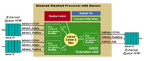
Figure 5. Example of Use of Queues to Speed Data Transfer.
Dual Load/Store Units for High-Speed DSP
The Diamond Standard 545CK includes two load/store units that can be used simultaneously, allowing the processor to perform XY memory operations, permitting very high performance execution of many DSP algorithms.
Interrupts and Timers
Unlike many other 32-bit processor cores, the Diamond Standard processors feature rich interrupt and timer capabilities. Nine external interrupts, three timer interrupts, and two software interrupts are provided.
Architectural Building Blocks
The following blocks are included in all Diamond Standard processors:
- On-chip Debug (OCD) – used to access the internal, software-visible processor state through a JTAG port. OCD support includes: debug-mode entry through exception generation, access to all program-visible registers and memory locations, execution of any instruction that the processor can execute, modification of the program counter to jump to a desired code location, real-time debug, and a utility for returning to normal operating mode.
- RAM – the RAMS provide internal memory ports with address ranges within the processor’s address space and accessed with the same timing as cache. There are two optional RAMS: instruction RAM and one or two data RAMS.
- Timer interrupts – there are three timer interrupts, with one 32-bit read/write register that increments every clock cycle and thee 32-bit comparison registers that can generate level-1 interrupts or high-priority interrupts.
The following blocks are included in some Diamond Standard processors:
- 16-bit multiply and multiple-accumulate (MAC16) (in Diamond 323GP, 232L, 570T, 330HiFi, and 545CK) – adds a 16x16-bit multiplier and a 40-bit accumulator, eight 16-bit operand registers (separate from the main register file), special load instructions for operand registers, and a set of compound operations. The MAC16 operand registers can be loaded with pairs of 16-bit values from memory in parallel with MAC16 operations and the MAC16 can sustain algorithms with two loads per multiply/accumulate.
- 32-bit Multiply (in Diamond 570T) – provides instructions that perform 32x32-bit multiplication, producing a 32-bit result.
Low Power – Built In
Clock gating is a very effective power reduction technique that reduces power by stopping unnecessary clocking activity to parts of the logic that are not in use on a particular clock cycle. Tensilica has designed fine-grained clock gating for every functional element of these processors. The Diamond Standard Series processor architecture dramatically lowers power consumption since it is designed to use power very efficiently.
Summary
The Xtensa architecture makes a number of fundamental contributions to embedded processor architecture, including:
- A full 16-visible windowed register file, three-operand programming model in less than 32-bit instruction encoding for performance, generality, and code size
- Rich selection of commonly occurring instruction combinations as compound instructions
- Encoding of common immediate values for performance and code-size
- An unusually rich and powerful branch architecture, including compare and branch, bit-test branches, coprocessor condition codes and branches, and zero-overhead loops, for performance and code size
- An available 16-bit instruction subset that can be freely intermixed with 24-bit base instructions for further code density improvement
The Diamond Standard Processors
The Diamond Standard 108Mini RISC Controller Core
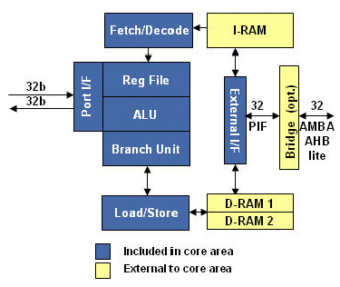
The Diamond Standard 108Mini is an efficient, ultra-low power, fully synthesizable 32-bit RISC CPU controller core.
Features include:
- Cacheless design with memory protection unit
- Single-cycle instruction and dual-data SRAM interfaces
- Non-maskable interrupt
- 9 external interrupts
- 3 timers
- On-chip debug hardware
- Programmable I/O ports reduce external control logic and speed I/O
- FPGA system prototyping support reduces design risk
- Deterministic real-time operation through optional single-cycle local instruction and/or data SRAM
- Optional AMBA AHB-lite interface
Representative Performance/Area/Power for Diamond 108Mini
| Maximum Frequency (0.13G worst case) | 233-250 MHz |
| Dhrystone 2.1 MIPS/MHz | 1.2 |
| Die Area (0.13G pre-layout)* | 0.43 mm2 |
| Die Area (0.13G post-layout)** | 0.51 mm2 |
| Instruction Width | 16/24 bits |
| mW/MHz (0.13G)** | 0.082 |
All area, power, and frequency numbers are representative only and subject to variation based on each user’s chosen process technology, cell library and design tools.
* Area is post synthesis, pre-layout
** Area and power are post synthesis, post clock tree insertion, assuming 85% utilization.
Diamond 108Mini Offers ARM9 Performance at ARM7 Power
| ARM 7TDMI-S** | Diamond 108Mini | ARM 968E-S | |
| Max frequency (0.13u G) worst case, optimized for speed | 146 MHz | 233-250 MHz | 240 MHz |
| Dhrystone MIPS | 131 | 300 | 264 |
| Power – mW per MHz (0.13G)* | 0.10 | 0.082 | 0.11 |
| Area – post synthesis | 0.24mm2** | 0.40 mm2 | 0.40 mm2 |
| Area – post layout | n/a | 0.51 mm2 | n/a |
| Number of interrupts | 3 | 15 | 3 |
| Timers | No | Yes | No |
| Direct interface ports/wires | No | 32-bit input ports, 32-bit output ports | No |
*Power depends on operating conditions, standard cell libraries, performance targets, and processor load.
**Assumes no bus interface, interrupt controller, trace interface, memory protection unit, GPIO. Data on ARM products taken from ARM public website, October 2006, for TSMC 0.13G process. All speed, power and area metrics are subject to variation based on user's design and fab choices.
The Diamond Standard 212GP Controller Core
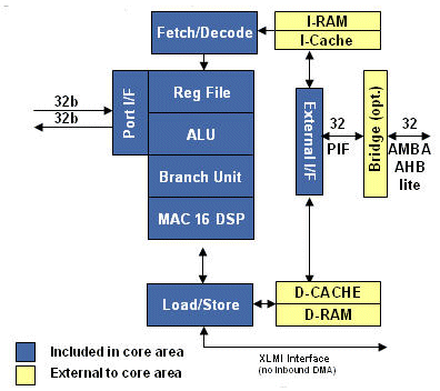
The Diamond Standard 212GP is a high-performance, versatile 32-bit RISC SOC controller core.
Features include:
- Single-cycle 16x16-bit MAC
- DSP instructions eliminate need for extra DSP
- 8Kbyte, 2-way set associative instruction and data caches, programmable write-through or write-back
- Local single-cycle instruction and data SRAM interfaces
- On-chip debug hardware
- Non-maskable interrupt
- 9 external interrupts
- 3 timers
- Programmable I/O ports reduce external control logic and speed I/O
- FPGA system prototyping support reduces design risk
- Optional AMBA AHB-lite interface
- 128-bit XLMI single-cycle bus that can perform transfers much faster than the main bus
- Zero-overhead looping to execute loops without stalls
Representative Performance/Area/Power for Diamond 212GP
| Maximum Frequency (0.13G worst case) | 233-250 MHz |
| Dhrystone 2.1 MIPS | 325 |
| Die Area (0.13G pre-layout)* | 0.56 mm2 |
| Die Area (0.13G post-layout)** | 0.77 mm2 |
| Instruction Width | 16/24 bits |
| mW/MHz (0.13G)** (power) | 0.116 |
All area, power, and frequency numbers are representative only and subject to variation based on each user’s chosen process technology, cell library and design tools.
* Area is post synthesis, pre-layout
** Area and power are post synthesis, post clock tree insertion, assuming 85% utilization.
Diamond 212GP Provides Better Performance than ARM9 with Lower Power and Smaller Area
| ARM 946E-S | Diamond 212GP | |
| Max frequency (0.13u G) worst case, optimized for speed | 210 MHz | 233-250 MHz |
| Dhrystone MIPS | 231 | 335 |
| Power – mW per MHz (0.13G)* | 0.31 | 0.116 |
| Area – post synthesis | 0.97 mm2 | 0.56 mm2 |
| Area – post layout | n/a | 0.77 mm2 |
| Zero-overhead looping | No | Yes |
| Number of interrupts | 3 | 15 |
| Timers | No | Yes |
| Direct interface ports/wires | No | 32-bit input ports, 32-bit output ports |
*Power depends on operating conditions, standard cell libraries, performance targets, and processor load.
Data on ARM products taken from ARM public website, October 2006, for TSMC 0.13G process. All speed, power and area metrics are subject to variation based on user's design and fab choices.
The Diamond Standard 232L RISC Controller Core
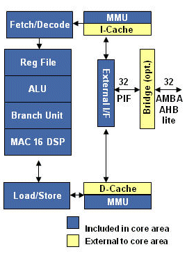
The Diamond Standard 232L is similar to the Diamond 212GP, but it adds a full-featured Memory Management Unit (MMU) for the Linux operating system.
Features include:
- Single-cycle 16x16-bit MAC
- DSP instructions eliminate need for extra DSP
- 8Kbyte, 2-way set associative instruction and data caches, programmable write-through or write-back
- On-chip debug hardware
- Non-maskable interrupt
- 9 external interrupts
- 3 timers
- Programmable I/O ports reduce external control logic and speed I/O
- FPGA system prototyping support reduces design risk
- Optional AMBA AHB-lite interface
- 128-bit XLMI single-cycle bus that can perform transfers much faster than the main bus
- Zero-overhead looping to execute loops without stalls
- Linux-compatible Memory Management Unit
Representative Performance/Area/Power for Diamond 232L
| Maximum Frequency (0.13G worst case) | 233-250 MHz |
| Dhrystone 2.1 MIPS | 300 |
| Die Area (0.13G pre-layout)* | 0.70 mm2 |
| Die Area (0.13G post-layout)** | 0.81 mm2 |
| Instruction Width | 16/24 bits |
| mW/MHz (0.13G)** (power) | 0.189 |
All area, power, and frequency numbers are representative only and subject to variation based on each user’s chosen process technology, cell library and design tools.
* Area is post synthesis, pre-layout
** Area and power are post synthesis, post clock tree insertion, assuming 85% utilization.
Diamond 232L Offers More Linux-Ready Features at Half the Power and Area
| ARM 926EJ-S | Diamond 232L | |
| Max frequency (0.13u G) worst case, optimized for speed | 250 MHz | 233-250 MHz |
| Dhrystone MIPS | 275 | 300 |
| Power – mW per MHz (0.13G)* | 0.36 | 0.189 |
| Area – post synthesis | 1.45 mm2 | 0.70 mm2 |
| Area – post layout | n/a | 0.77 mm2 |
| Zero-overhead looping | No | Yes |
| Number of interrupts | 3 | 15 |
| Timers | No | Yes |
*Power depends on operating conditions, standard cell libraries, performance targets, and processor load. Data on ARM products taken from ARM public website, October 2006, for TSMC 0.13G process. All speed, power and area metrics are subject to variation based on user's design and fab choices.
The Diamond Standard 570T Static-Superscalar Controller Core
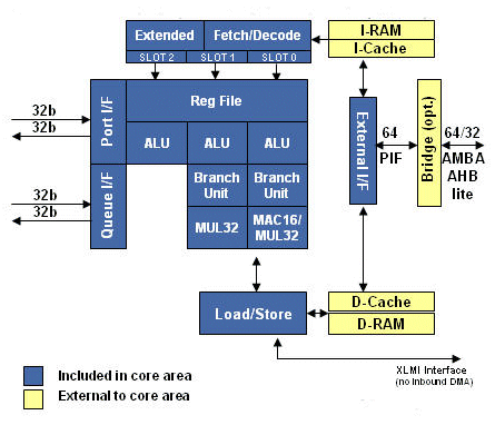
The Diamond Standard 570T is among the highest performance, highest throughput licensable embedded CPUs available today.
Features include:
- Three-issue, static superscalar VLIW CPU
- Modeless switching between 16-, 24-, and 64-bit 2- or 3-issue instructions
- 64-bit local memory interfaces to cache and single-cycle local SRAM
- Single-cycle 16x16-bit MAC and dual 32-bit multipliers
- 16Kbyte, 2-way set associative instruction and data caches, programmable write-through or write-back
- Single-cycle instruction and data SRAM interfaces
- On-chip debug hardware
- Non-maskable interrupt
- 9 external interrupts
- 3 timers
- Programmable I/O ports reduce external control logic and speed I/O
- FPGA system prototyping support reduces design risk
- Optional AMBA AHB-lite interface
- 128-bit XLMI single-cycle bus that can perform transfers much faster than the main bus
- 64-bit peripheral interface (PIF) bus
- High-speed 32-bit in/out queues eliminate main system bus data contention
Representative Performance/Area/Power for Diamond 570T
| Maximum Frequency (0.13G worst case) | 200-233 MHz |
| Dhrystone 2.1 MIPS/MHz | 1.52 |
| Die Area (0.13G pre-layout)* | 1.03 mm2 |
| Die Area (0.13G post-layout)** | 1.58 mm2 |
| Instruction Width | 16/24/64 bits |
| mW/MHz (0.13G)** Power | 0.087-0.410 |
| mW/MHz (90nm typical max frequency)** (power) | 0.155 |
All area, power, and frequency numbers are representative only and subject to variation based on each user’s chosen process technology, cell library and design tools.
* Area is post synthesis, pre-layout
** Area and power are post synthesis, post clock tree insertion, assuming 65% utilization.
Diamond 570T Uses Less than Half the Die Area and Power of ARM 1136/1156
| ARM 1156T2-S | Diamond 570T | ARM 1136J-S | |
| Instruction Issue (per cycle) | 1 | 3 | 1 |
| Dhrystone MIPS | 402 | 354 | 396 |
| Dhrystone MIPS/MHz | 1.20 (est) | 1.52 | 1.20 |
| Power – mW per MHz (0.13G)* | 0.24 | 0.08 | 0.24 |
| Area – post layout | 0.90 mm2 | 0.48 mm2 | 0.90 mm2 |
| Number of pipeline stages (deeper pipelines are less efficient) | 9 | 5 | 8 |
| Instruction width | 16/32 bit | 16/24/64 bit 3-issue | 16/32 bit |
| High throughput data Queues | No | Yes (input and output) | No |
| Direct interface ports/wires | No | 32-bit input ports, 32-bit output ports | No |
*Power depends on operating conditions, standard cell libraries, performance targets, and processor load.
Data on ARM products taken from ARM public website, October 2006, for TSMC 90nmG process. All speed, power and area metrics are subject to variation based on user's design and fab choices.
The Diamond Standard 330HiFi Audio Engine
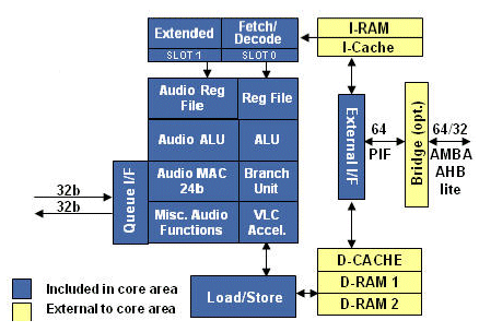
The Diamond 330HiFi core is optimized for digital audio processing. All popular audio codecs have been pre-ported to the Diamond 330HiFi core, making it a “drop-in” block for any SOC application requiring high-quality 24-bit audio.
Features include:
- Dual-issue, static superscalar VLIW CPU
- Modeless switching between 16-, 24-, and 64-bit dual-issue instructions
- 64-bit local memory interfaces to cache and single-cycle local SRAM
- Dual MACs can operate as 32x16-bit or 24x24-bit
- 4Kbyte instruction and 8Kbyte data 2-way set associative caches, programmable write-through or write-back
- Single-cycle instruction and data SRAM interfaces
- On-chip debug hardware
- Non-maskable interrupt
- 9 external interrupts
- 3 timers
- FPGA system prototyping support reduces design risk
- Optional AMBA AHB-lite interface
- 64-bit peripheral interface (PIF) bus
- High-speed 32-bit in/out queues eliminate main system bus data contention
- Single audio engine supports multiple codecs
- Performance headroom to perform other functions
- Full 24-bit internal audio resolution for high-quality audio
Representative Performance/Area/Power for Diamond 330HiFi
| Maximum Frequency (0.13G worst case) | 200-233 MHz |
| Dhrystone 2.1 MIPS/MHz | 1.3 |
| Die Area (0.13G pre-layout)* | 1.33 mm2 |
| Die Area (0.13G post-layout)** | 2.04 mm2 |
| Instruction Width | 16/24/64 bits |
| mW/MHz (0.13G)** Power | 0.089-0.352 |
| mW/MHz (90nm typical max frequency)** (power) | 0.148 |
All area, power, and frequency numbers are representative only and subject to variation based on each user’s chosen process technology, cell library and design tools.
* Area is post synthesis, pre-layout
** Area and power are post synthesis, post clock tree insertion, assuming 65% utilization.
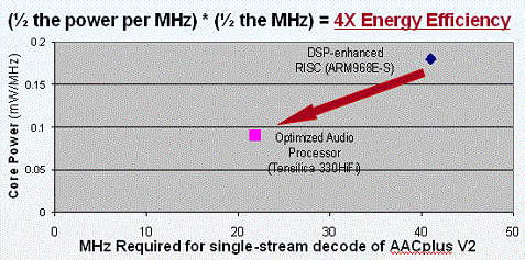
Diamond 330HiFi is Four Times as Energy Efficient as ARM968E-S
Diamond Standard 545CK 8-MAC, VLIW DSP
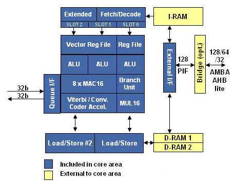
The Diamond 545CK is the highest performance licensable DSP IP core. It is a single core that can be used for both system control and DSP.
Features include:
- Highest performance and efficiency of any licensable DSP core
- Three-issue, static superscalar VLIW
- Modeless switching between 16-, 24-, and 64-bit three-issue instructions
- Up to 8 MAC operations per cycle
- 16 x 160-bit vector registers
- Two 128-bit load/store units
- 64 general purpose registers
- Viterbi accelerator
- Support for other DSP operations: saturated arithmetic, max/min value, normalize, sign extend, etc.
- Single-cycle instruction and dual data SRAM interfaces
- On-chip debug hardware
- Non-maskable interrupt
- 9 external interrupts
- 3 timers
- FPGA system prototyping support reduces design risk
- Optional AMBA AHB-lite interface
- 128-bit peripheral interface (PIF) bus
- High-speed 32-bit in/out queues eliminate main system bus data contention
Representative Performance/Area/Power for Diamond 545CK
| Maximum Frequency (0.13G worst case) | 233-250 MHz |
| Dhrystone 2.1 MIPS/MHz | 1.52 |
| Die Area (0.13G pre-layout)* | 1.03 mm2 |
| Die Area (0.13G post-layout)** | 1.58 mm2 |
| Instruction Width | 16/24 bits |
| mW/MHz (0.13G)** Power | 0.087-0.410 |
| mW/MHz (90nm typical max frequency)** (power) | 0.155 |
All area, power, and frequency numbers are representative only and subject to variation based on each user’s chosen process technology, cell library and design tools.
* Area is post synthesis, pre-layout
** Area and power are post synthesis, post clock tree insertion, assuming 50% utilization.
Diamond 545CK is the Fastest Licensable DSP Core
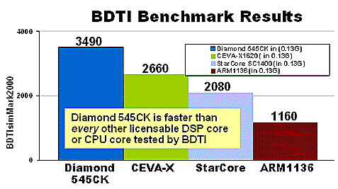
BDTI BenchmarksTM Notes:
All scores use worst-case clock speeds for the TSMC CL013G process and ARM Artisan SAGE-X library.
The BDTIsimMark2000TM is a summary measure of DSP speed. See www.BDTI.com for info. Scores © 2006 BDTI.
Diamond 545CK configuration tested by BDTI: 220 MHz final layout timing under worst case conditions. 3.7 mm2 actual layout area. Leakage power 0.7mW + dynamic power 0.2 mW/MHz.
Benchmarks – The Diamond Standard Processor Family Xtensa-Based Architecture Tops Industry Leaders
In benchmark after benchmark, the Diamond Standard processor family comes out on top. Tensilica used its Diamond 570T high-performance CPU in the popular industry EEMBC benchmarks, and here are the results.
EEMBC (Embedded Processor Benchmark Consortium) Benchmarks
No single benchmark can accurately capture the full range diversity of embedded applications. In an effort to create an embedded benchmark that would be more informative than the Dhrystone, EDN Magazine sponsored the creation of a comprehensive suite of representative embedded applications. More than 40 leading processor and software companies have joined EEMBC and together developed both a set of benchmarks and a fair process for running, measuring, certifying, and publishing test results. These benchmarks cover a wide range of embedded tasks, but the bulk of the certified results are available for four suites: networking, consumer, telecommunications, and office automation.
The data in this section is taken directly from the certified results on the EEMBC website at www.eembc.com, as of October 2006. In each case we compare the Diamond Standard 570T processor core to the ARM cores
The ARM architecture is represented in the EEMBC benchmarks by the ARM1026EJ-S, the only core that has been benchmarked by ARM. We also compare it to the ARM1136JF-S, which was benchmarked in a Freescale IMX31 device. No certified ARM11 EEMBC results have been published as of October 2006.
Each EEMBC test suite consists of a number of different programs, written in C. The EEMBC Netbench 1.1 benchmark suite approximates the performance of processors in low-end routers. It consists of three benchmark kernels. One implements the Dijkstra shortest-path-first algorithm, which is widely used in routers and other networking equipment to find the shortest or least-cost path from a specific router to all other routers. The packet flow benchmark indicates the potential performance in an IP router with four network interfaces. In the route look-up benchmark, performance is measured on the fundamental operation of IP datagram routers, including receiving and forwarding IP datagrams and implementing an IP lookup mechanism based on a Patricia Tree.
The EEMBC Consumer benchmark suite is a compilation of five separate benchmark kernels that are representative of consumer digital imaging applications. The high-pass grey-scale filter benchmark demonstrates performance in front-end processing of digital still cameras, showcasing 2-D data array and multiply/accumulate capabilities. The JPEG compression and decompression benchmarks take still images from full source data captured from a sensor, compress to a JPEG file format for data storage, and reconvert back to full image representation, a common set of tasks in consumer products such as digital still cameras and digital video camcorders. The RGB to CYMK conversion benchmark demonstrates a common conversion used in color printing. The RGB to VIQ conversion benchmark demonstrates a conversion used in NTSC encoders for digital video processing.
The EEMBC Office Automation benchmark is a suite of benchmarks that approximate the performance of processors in printers, plotters and other office automation systems that handle text and image processing text. It includes a dithering benchmark that evaluates how the processor handles indirect references (used for managing internal buffers), how it manipulates large data sets, how it manipulates packed-byte quantities (used to hold gray-scale pixel data), and how it performs four byte-wide multiply accumulate operations per pixel. An image rotation benchmark uses a bitmap rotation algorithm that rotates a complete binary image 90 degrees clockwise, testing bit manipulation, comparison and indirect reference capabilities. A text processing benchmark exercises the processor’s byte manipulation, pointer comparison, indirect reference handling, and stack manipulation capabilities.
The EEMBC Telecom benchmark suite approximates the processor’s performance in modem, xDSL, and related fixed-telecom applications. It includes five kernels that represent traditional DSP algorithms. The autocorrelation benchmark is based on a mathematical tool used frequently in signal processing for analyzing functions or series of values, such as time domain signals. The convolutional encoder benchmark, useful for cellular and modem applications, adds redundancy for error checking and explores the ability to perform bit-wise exclusive ors and table lookups. The bit allocation benchmark test the ability to stream data over a series of buffers, which it then modulates and transmits on a telephone line in ADSL applications. The Inverse Fast Fourier Transform benchmark tests the ability to convert frequency domain data into time domain data. The Fast Fourier Transform benchmark tests the ability to convert time domain data into frequency domain data. And the Viterbi decoder benchmark tests the processor’s ability to recover an output data packet from an encoded input data packet in embedded IS_136 channel coding applications.
The following chart shows that the Diamond Standard 570T performs much better than any ARM processor tested.
Diamond 570T Performs 2.3X BETTER than ARM1136JF-S on EEMBC Benchmarks
| ARM 1136JF-S* | ARM 1026EJ-S (certified as a core) | Diamond 570T | |
| NetMARK | 1.0 | 1.29 | 2.55 |
| ConsumerMARK | 1.0 | 1.47 | 2.91 |
| OfficeMARK | 1.0 | 1.19 | 1.64 |
| TeleMARK | 1.0 | 1.06 | 2.28 |
| Geometric Mean | 1.0 | 1.24 | 2.30 |
*Results extrapolated from Freescale IMX31 device. No certified ARM1136JF-S EEMBC results have been published as of October 2006.
Related Semiconductor IP
- NPU IP Core for Mobile
- NPU IP Core for Edge
- Specialized Video Processing NPU IP
- HYPERBUS™ Memory Controller
- AV1 Video Encoder IP
Related White Papers
- IP Processor Core Platform Selection According to SoC Architecture: a case study
- SoC Test and Verification -> Assertions speed processor core verification
- High-Performance DSPs -> Processor boards: Architecture drives performance
- An Embedded Processor Architecture With Extensive Support For SoC Debug
Latest White Papers
- Ramping Up Open-Source RISC-V Cores: Assessing the Energy Efficiency of Superscalar, Out-of-Order Execution
- Transition Fixes in 3nm Multi-Voltage SoC Design
- CXL Topology-Aware and Expander-Driven Prefetching: Unlocking SSD Performance
- Breaking the Memory Bandwidth Boundary. GDDR7 IP Design Challenges & Solutions
- Automating NoC Design to Tackle Rising SoC Complexity