Design Rule Checks (DRC) - A Practical View for 28nm Technology
Vipul Patel, einfochips ltd
Abstract
The main objective of this paper is to explain the various types of design rule checks (DRC) violation, their causes and how to fix the various design rule checks (DRC) at lower technology node on block level as well as full chip level implementation while meeting the design rule with respect to latest technology standards.
I. INTRODUCTION
The first question that comes to the mind of an ASIC designer is “what is a design rule check?”, why we are doing this at SOC level, and what would happen if the design does not meet the design rule checks? In this paper, you will find the answer to all these queries. Design rule checks are nothing but physical checks of metal width, pitch and spacing requirement for the different layers which depend on different technology nodes. We need to clean up the DRC of the design because there is a logical connection of various components, and if they are physically connected, then it will fail the functionality of the chips, and chips won’t be able to perform a specific task.
The layout of a design must be in accordance with a set of predefined technology rules given by the foundry for manufacturability. After completion of the layout and its physical connection, an automatic program will check each and every polygon in the design against these design rules and report any violations. This whole process is called Design Rule Checking (DRC). There are many design rules at different technology nodes, a few of which are mentioned below.
Types of DRCs:
- Minimum width and spacing for metal
- Minimum width and spacing for via
- Fat wire Via keep out Enclosure
- End of Line spacing
- Minimum area
- Over Max stack level
- Wide metal jog
- Misaligned Via wire
- Different net spacing
- Special notch spacing
- Shorts violation
- Different net Via cut spacing
- Less than min edge length
Here are some of the practical problems and their solution for different types of DRCs and their solutions.
CASE A: Shorts violation
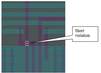
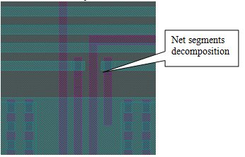
Description: In short violation, two or more different net segments of the same layer were crossing each other. Here is a practical problem of two different nets in same metal layer crossing to each other as seen in the following pic.
Solution:
To fix this type of short violation, different net segments on same layer has to be placed away so that they will not cross each other. In this case, net adjusted net will not cross each other and also meet the spacing requirement in the same layer.
CASE B: Different Spacing violation
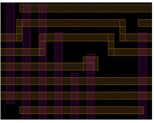
Description : In some cases, the via enclosure is quite large compared to metal width due to large via enclosure. Thee other long net passing each other and dropped in via will create a different spacing violation.

Solution:
To fix this type of spacing violation, the net needs to be placed away from the via, or different size vias need to be inserted so it will meet the same net spacing requirement. In above case, routing taken in reverse U shape will meet the spacing requirements as below.
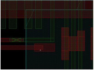
CASE C: Same layer spacing with net and cell geometry blockage
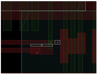
Description: In this case, there is same layer spacing with the cell blockage and via enclosure
Highlighted in pic using white marker. Same net spacing in red color.
Solution:
In this case, to fix violation, the net is routed in non-preferred direction in green color inserted via so spacing is increased between cell blockage and a net.
CASE D: Minimum area requirement
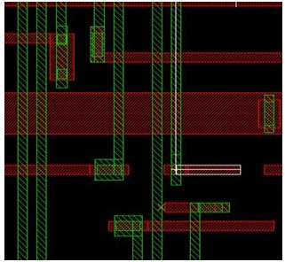
Description: There is a minimum area requirement for every segment in a layout.

Solution:
To meet this minimum area requirement, we need to increase the area of the segment that will not violate the other design rule (spacing, short). For this case I have increase the area where I was getting the violation shown below.
CASE E: VIA Misalignment
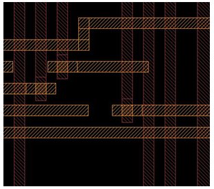
Description: This type violation pops up when two different layer of same logical net connected by inserting the VIA. If inserted via is not aligning with the metal crossing we are seeing the VIA misalignment.

Solution:
Proper VIA instance need to insert so the VIA enclosure align layer in its direction properly and if needed we need to stretch the net and insert the VIA.
After fixing the all DRC again we need to verify drc with different tool Caliber,Quartz before releasing to foundary because while fixing the drc there may be a chances of populating the new DRC violation.
Author
Vipul Patel, Senior Engineer (einfochips ltd)
Experience in Place & Route, Static Timing Analysis, and Layout Verification, Signal Integrity analysis, Low power technique implementation.
I’m a physical design engineer with 5 years experience in Very Large Scale Integration/Application Specific Integrated Circuits field, I have worked on different nanometer technology node (16nm,28nm,40nm,65nm) of ASIC design Chips (SoC) in semiconductor industry from RTL netlist to GDS II, Sign off process. I have successfully taped out multiple SoC. I have handled many block which have more 2 million instance count with high number of SRAMS and successfully completed whole PnR (Placement to Route) to sign off flow. I have worked on different client project based on client requirement (High speed Router SoC, Low Power SoC, FPGA SoC, Different processor Series quadcore, octa core SoC ).
Related Semiconductor IP
- NPU IP Core for Mobile
- NPU IP Core for Edge
- Specialized Video Processing NPU IP
- HYPERBUS™ Memory Controller
- AV1 Video Encoder IP
Related White Papers
- A Heuristic Approach to Fix Design Rule Check (DRC) Violations in ASIC Designs @7nm FinFET Technology
- Design and implementation of a hardened cryptographic coprocessor for a RISC-V 128-bit core
- Customizing a Large Language Model for VHDL Design of High-Performance Microprocessors
- An FPGA-to-ASIC case study for refining smart meter design
Latest White Papers
- Ramping Up Open-Source RISC-V Cores: Assessing the Energy Efficiency of Superscalar, Out-of-Order Execution
- Transition Fixes in 3nm Multi-Voltage SoC Design
- CXL Topology-Aware and Expander-Driven Prefetching: Unlocking SSD Performance
- Breaking the Memory Bandwidth Boundary. GDDR7 IP Design Challenges & Solutions
- Automating NoC Design to Tackle Rising SoC Complexity