Design of Base I/O Libraries (by Ron Nikel, Co-Founder and CTO of TriCN)
Cell libraries clearly play a critical role in IC design today. They serve as the fundamental building blocks for any new chip design. Most developers have chosen a standard cell library early in the design process, frequently based on which IC foundry they are working with—and verified that the library works smoothly within their design flow.
When it comes to the evaluation and selection of a Base I/O library, however, things are not so cut-anddried. I/O libraries for chip designers present a challenging problem in the design process, made even more difficult with the move to smaller geometries and higher performance targets. These challenges involve the integration of the I/O design with standard and memory cells, and mixed-signal and analog blocks, which together constitute the chip under development.
Standard cells and memories are usually employed with little difficulty in a design flow, just as standard tools and methodologies have evolved for these types or circuits to ensure a smooth, well-understood design flow from register-transfer level (RTL) to GDS2. Such circuits typically exist in a single power domain and are easily modeled as a mixture of combinatorial and sequential logic.
I/O and mixed-signal circuits, by contrast, present a significantly greater challenge to electronic design automation (EDA) tools. I/O circuits are analog in nature and their digital equivalent behavior not easily modeled; signal delays through analog circuits can be quite complex to predict and model using today’s standard static timing tools.

In this age of ever increasing complexity of ICs and the interfaces that reside on them, there will likely be three (and often more) separate voltage supply domains on the chip. The need to accommodate multiple voltage supply domains compounds the challenges facing design tools and designers.
Chip packaging further adds to the design challenge. More than ever, chip designers are creating designs using flip chip packaging, which increases the complexity of the I/O integration into the overall chip design. (see sidebar—“The impact of IC packaging options on design libraries”)
Creating a I/O library with diverse functionality
IC designers are faced with interfacing to a growing diversity of standards and parts. I/Os that only work with 3.3V low-voltage transistor-transistor logic (LVTTL) are proving inadequate for today’s complex chips, chips that include interfaces to memory, I/O, graphics, and networking. These new chip designs must potentially work with a dizzying array of industry standards, such as double data rate (DDR) I and DDR II, synchronous dynamic random access memory (SDRAM), peripheral component interconnect (PCI) and its higher- performance PCI-X variant, quad data rate (QDR), static RAM (SRAM), Universal Serial Bus (USB).
Today’s I/O libraries are also required to support high-speed transceiver logic (HSTL) and stub series terminated logic (SSTL-2). Meanwhile, library should be scalable to include low-voltage differential signaling (LVDS), current-mode logic (CML), MDIO, along with phase-lock loops (PLLs), delay-lock loops (DLLs), and serializer-deserializers (SerDes) such as PCI-Express, XAUI (10-Gb attachment unit interface), System Packet Interface Level 4 (SPI-4.2), HyperTransport and Rapid I/O.
The list goes on and on! At the end of the day, a robust toolbox of off-the-shelf I/Os is needed to ensure that the chip designer spends more time developing good chip architecture and less time hunting around for the right I/O to interface to the rest of the system.
What happens, however, when a chip designer has no need for all theses higher, more-complex functions on a design? Why should a single library be asked to support all of this, if the need is not there?
The short answer is integration and scalability. If a pad ring is developed to support only the simplest of functions, its use in a later design built with the same low-performance cell library will make it difficult at best to include, for instance, a very sophisticated SerDes.
The message? If you’re working on a design that does not need high performance, and if the interfacing requirements are also fairly simple, a very basic I/O library may serve you well. But if at a later point, you want to leverage your design for higher performance, the cells you’ve used will limit you. It may take a great deal of re-engineering to get the existing design to work well at the higher speeds. All of the re-engineering work dilutes the benefits supposedly gained by “leverage”— the idea of re-purposing previous design work.
I/O libraries and tape-out kits
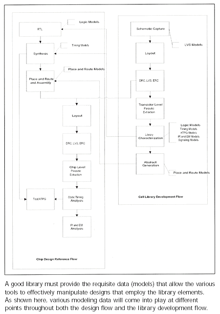
The real test of a good library is in how well it interfaces with standard tools from EDA companies. Faced with having to satisfy design rule checkers (DRC), layout-versus-schematic (LVS) checkers, static timing analyzers, Verilog simulators, chip place-and-route tools, IR drop analyzers, electromigration (EM) analysis, board-level signal integrity, and design-for-test analysis tools—library designers are challenged just to deliver a GDSII to the end user, much less all of the views needed for each of these various EDA tools in the flow. Nevertheless, it is incumbent upon the library developer to provide all required views to ensure that the library works well with all end-user chip design flows.
When designing and verifying a library for use by customers, the following EDA models must be generated in order to support the wide range of tools that might be employed by a user:
• Logic models (.v or .vhdl are examples)
• Timing models (.lib or .tlf are examples)
• Place-and-Route models (LEF or FRAME are examples)
• ATPG models (tetramax, fastscan, or LogicVision are examples)
• LVS models (spice, cdl, or edif are examples)
• Signaling models (SPICE or IBIS)
• IR-drop models (Simplex or Apache are examples)
• Electromigration models (Simplex or Apache are examples)
Importantly, these models must be functional with the EDA tools for which they are intended. The models must also be self-consistent, so that the handoff of databases as chip design proceeds from RTL to GDS adds to a seamless analysis of the design. For instance, it’s important that a logical netlist that instantiates a cell can be annotated at a later point in the design with timing information from the timing model.
Among the issues specifically addressed in the I/O library is the logical models that implement analog power and ground domains, and I/O power and ground domains. This is particularly important when designing a chip that has more than one power domain. In many design flows, chip-level LVS netlists are generated from the logical netlist—in many cases, a Verilog netlist. Most chips today have more than three separate power domains. (see Figure)
Typically in the past, place-and-route tools have not handled I/Os well, but the size and complexity of today’s designs have forced a considerable improvement in these tools. In order for such tools to place the I/Os correctly and to run automatic verification and routing for these circuits, complete routing views—with core, I/O and analog power pins correctly detailed—must be available, so that the router handles the hookup correctly. The only way this can be guaranteed is if the library developer builds a reference chip design using the tools the customer would be using. At TriCN, we not only build a reference chip design using our library, but also provide the design to the customer, so that the customer has the tool setup files as a basis for developing their own chips.
As clock frequencies and power dissipation levels increase, new tools have emerged to analyze on-chip power supply IR drops. Analysis at the chip level requires a model that represents the current and physical interconnect of each cell in the library. This information is represented in the database used to model the current flow throughout the chip, showing areas that are currentstarved or areas of high current density. This type of analysis can be used to change the power distribution on-chip, thereby increasing reliability (by reducing electromigration), or improving IR drop (to ensure that critical circuits operate at speed). The I/O database is particularly important in this process — all power to the chip is provided through the I/O cells — and for very high-performance cells, the largest DC current draw is typically in the I/Os themselves.
Another very important but overlooked point is the ability to combine the I/O library with libraries for standard cells, memories and analog components, in order to create a full chip design using a common EDA platform. In developing the TriCN I/O library, we ran reference design test cases using library platforms provided by other IP providers, to ensure that our I/O library is compatible with cell libraries from other suppliers. This, in turn, ensures ease-of-use for our customers.
Libraries that meet the challenge
I/O is essentially analog in nature and analog circuits can be difficult to model, as well as sensitive to geometry and process changes. There is an ever-growing proliferation of I/O standards in use today. Developing an I/O library that can handle all these issues—and also work smoothly with a wide variety of EDA tools—can therefore present a stiff challenge. For chip designers who must identify and qualify the right I/O library for their target design, the challenges are intense as well.
It pays, therefore, to analyze what type of designs you are working on and what you may be working on in the future. Some designers simply want to get data on and off the chip, with no particular emphasis on performance level. Many of the libraries that have been on the market for some time are able to support that class of requirement. But as device geometries shrink, and as performance targets increase, designers are facing more and more engineering development effort to modify the libraries to support required performance targets. For some customers, there is indeed a new demand for a higher-performance base I/O library, available right of the box, capable of supporting today’s complex designs.
Bio
Ron Nikel is Co-Founder and Chief Technology Officer of TriCN (founded in 1997). Previously, he worked at Digital Equipment Corporation, specializing in circuit design and signal integrity on the VAX 10000 and DEC 7000 servers. Prior to DEC, Nikel served at Silicon Graphics as a circuit interconnect technologist for the Origin 2000 program, and developed the Craylink technology and the copper 500Mb/s and the 1Gb/s optical interface for the HIPPI-6400- PH standard.
The impact of IC packaging options on design libraries
There are two extremes in chip development: low-cost packaging which supports low pin counts and relatively high-cost packaging which supports high pin counts. At these two extremes, the packaging die attach mechanisms are bondwire and flip chip, respectively. Each packaging type presents a challenge that needs to be addressed in the I/O library.
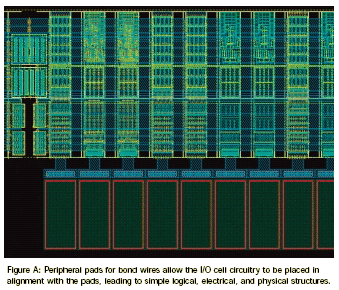
With bondwire-attached chips, the I/O cells are placed at the edge of the die. The I/Os themselves are decoupled from the core circuitry by isolation structures, to ensure that electrical noise is not coupled into the core. Additional circuitry—for latch-up and electrostatic discharge (ESD) protection— is placed within the cells that together form a ring around the edge of the die that is called the I/O pad ring. The bondwire pads are placed at the very edge of the die, outside of the I/O circuitry. This type of structure is typical to ICs and that which chip designers are most familiar with. (See Figure A)

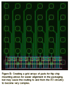
The flip chip is emerging today, however, as the more common form of chip-to-package attachment. In this scenario, instead of placing the pads at the edge of the die, the pads are arrayed across the face of the die. The I/O circuits can then be placed either at the edge of the die (as in traditional design, with bond-wire die) or they can be placed inside the core of the chip along with the rest of the core logic. The top level of metalization is then used to connect the I/O circuitry itself to the flip chip pads. The pads are, in turn, connected to the package through a solder ball in much the same way that a ball grid array (BGA) package is connected to a printed circuit board (PCB). (See Figure B)

The main challenge in designs using flip-chip packaging lies in the fact that the circuits responsible for latchup, ESD, and isolation now have to be implemented in a new way. The I/O circuitry must be placed next to critical combinatorial circuits and memories in the core.
If an I/O library is to properly support both bondwire and flip chip applications, therefore, it must be able to individually isolate each I/O cell from surrounding circuits, and ensure that switching noise from I/O cells does not couple into sensitive neighboring circuitry. Similarly, the library must implement a distributed ESD and latchup circuitry mechanism, one that not only protects I/O circuits when they are placed in a ring at the edge of the chip, but also offers protection when such circuits are placed in smaller groups in the core of the chip.
Related Semiconductor IP
- NPU IP Core for Mobile
- NPU IP Core for Edge
- Specialized Video Processing NPU IP
- HYPERBUS™ Memory Controller
- AV1 Video Encoder IP
Related White Papers
- Bigger Chips, More IPs, and Mounting Challenges in Addressing the Growing Complexity of SoC Design
- Design and Implementation of Test Infrastructure for Higher Parallel Wafer Level Testing of System-on-Chip
- Design and implementation of a hardened cryptographic coprocessor for a RISC-V 128-bit core
- A Survey on the Design, Detection, and Prevention of Pre-Silicon Hardware Trojans
Latest White Papers
- Transition Fixes in 3nm Multi-Voltage SoC Design
- CXL Topology-Aware and Expander-Driven Prefetching: Unlocking SSD Performance
- Breaking the Memory Bandwidth Boundary. GDDR7 IP Design Challenges & Solutions
- Automating NoC Design to Tackle Rising SoC Complexity
- Memory Prefetching Evaluation of Scientific Applications on a Modern HPC Arm-Based Processor