CPF Based Verification of an SoC - Lessons Learnt
Baris Guven, Levent Cetrez (Ericsson Microelectronics Design Center)
Abstract :
Power Management keeps being a very valuable asset for mobile applications. CPF (Common Power Format) is a common file format to describe the power structure of the design in the early design stages that makes it a very critical design step input of the VLSI design flow. It is possible to verify a design from low power point of view using lint tools [1,2] and/or simulations without CPF, but not as effective as a CPF based simulation methodology.
The aim of this paper is to introduce different design architectures to illustrate how CPF based verification works and points out the strengths and weaknesses of the methodology. All architecture examples mentioned in the paper are taken from a real SoC design that is produced and verified to be working on silicon.
Keywords—Common Power Format, Power Domain, Low Power, CPF based Verification
I. INTRODUCTION
OWER consumption is extremely important in today’s complex SoCs that are targeted for low power applications such as mobile phones. For this reason, to save power, SoCs are splitted into multiple power domains where supply of the logic inside the power domain can be shut off entirely when not needed. Designing multi power domain SoCs bring extra design requirements that needs to be carefully implemented. In order to address multi power domain design requirements, CPF methodology [3,4] is widely used for SoCs that contain multiple power domains. The methodology enables designers to do power aware design for multi power domain SoCs and detect potential design problems at early design stages. The design examples in this paper are similar to the ones in a real SoC project that is proven to be working on silicon. The first cuts of the SoC were designed without using a CPF methodology because of the fact that the design flow was not supporting CPF at that time. The last cuts were done using CPF methodology. Due to this difference in design methodology between cuts, we were able to judge the usefulness of the CPF based verification methodology [5,6,7,8] effectively.
II. SOC POWER DOMAINS
The SoC design was divided into three power domains as shown in Figure 1.
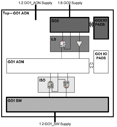
Fig. 1. Power Structure of the design.
GO2 region is supplied with 1.8 V VDD_IO that is always available even when the chip is in reset mode. GO1_AON region is supplied with 1.2V VDD_GO1_ON and is powered a defined time after chip reset is released. GO1_SW region is supplied with 1.2V VDD_GO1_SW and is powered only when the chip is in active mode for performing the core functionality of the chip. In sleep mode, this region is closed.
There are level shifters for all signal crossings from GO1_On to GO2 power domain and vice versa due to voltage differences between two power domains. Isolation cells are inserted between the signals that are crossing from GO1_SW to GO1_AON region. GO1_AON and GO1_SW power supplies are controlled by enable signals that are generated by a state machine. State machine also generates enable signals for level shifters and isolation cells.
III. DESIGN METHODOLOGY DIFFERENCES WITH AND WITHOUT USING CPF
The main difference between cuts that did not use CPF and the ones that used CPF was in the verification phase. CPF methodology enables doing verification with logic simulators by providing a CPF based text file that describes the power domain specification of the SoC design. By doing a CPF based verification, the simulator propagates unknown (also called ‘X’) values from all signals from the shut-off domains imitating real life behaviour. This allows designers to do verification more accurately. In the first cuts, since a CPF methodology was not used, even if the power domain was shut off, there were still defined logic values that were propagating from the shut off domain. This can result in false real time behaviour of the design. As a result of this false behaviour, real design problems can be overshadowed. This article will cover such an example how CPF is very good at finding such problems that could not be found with the first cuts which did not use CPF verification methodology. It will also introduce an example to show that CPF methodology can sometimes be too pessimistic and can point to design problems that are not real.
All the examples presented in this paper are related to potential issues at chip startup phase (i.e. when there is power at GO2 region and master chip reset is released). Since the verification without CPF can not model shut-off regions properly, this kind of problems can not be seen with a logic simulator.
IV. LEVEL SHIFTER ENABLE GENERATION LOGIC
Due to voltage difference between two domains, level shifters are inserted between GO1_AON and GO2 regions. When GO1_AON region is off, the level shifters also need to do the isolation from GO2 region as well. For this reason, all the level shifters from GO1_AON to GO2 region have an active high enable signal. When the enable signal is high, the input GO1_AON 1.2V signal is converted to output GO2 1.8V signal. When the enable signal is low, the level shifter output is forced to logic 0 stating that the GO1_AON region is off. Level shifter enable generation logic is shown in Figure 2.
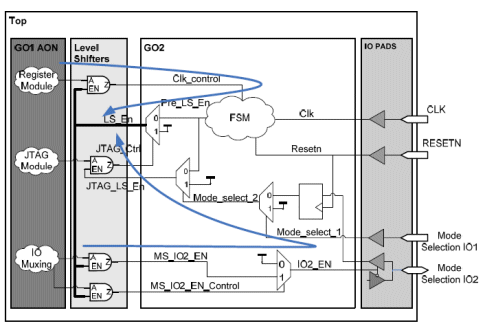
Fig. 2. Level shifters’ enable generation logic.
It is required for the level shifter enable logic to be directly controlled through GO2 region since GO2 voltage is always available. That is the case in Figure 2. However, a closer look to the diagram shows that although level shifter enable is generated in GO2 region, part of the logic that is generating the enable signal is coming from GO1_AON region after passing through other level shifters as shown by arrows. Moreover, the enable signal of those level shifters is controlled through the same level shifter enable. This creates a situation where level shifters’ enable signal generation is depending on the logic which is coming from the level shifter outputs that are controlled by the same level shifter enable. At start up, the enable signal generation logic causes a design issue that should be avoided because the level shifter enable logic creates a loop. Enable is dependent on couple of signals that are also depending on the level shifters’ outputs that are controlled by the enable itself.
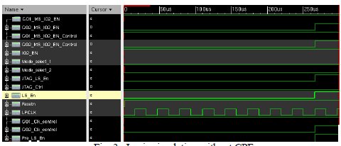
Fig. 3. Logic simulation without CPF.
Unfortunately, this design problem can not be seen in simulations where CPF is not used. Figure 3 shows the waveforms of the logic simulation without CPF usage. It can be seen that the signals that are coming from GO1_AON region when this region is powered down at start up are all defined and not shown as ‘X’. This logic simulation shows a clean result where level shifter enable signal (LS_En) can be generated successfully.
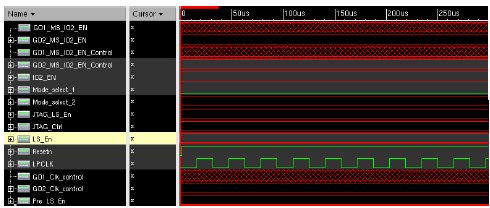
Fig. 4. Logic simulation with CPF.
On the other hand, Figure 4 shows the same simulation but this time a CPF file is used. In this case, it is seen that level shifter enable signal (LS_en) can not be generated successfully. This causes the simulation to fail. It can be seen from the simulation with CPF that when GO1_AON region is off, the signals from that region are propagating all ‘X’s. Since level shifter enable is depending on those signals, it becomes undefined as well. As a result, the circuit can never recover from the undefined level shifter enable situation.
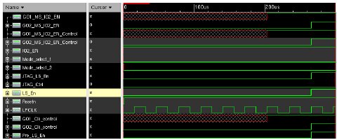
Fig. 5. Logic simulation with CPF and level shifter outputs are forced at start-up.
Figure 5 shows the case where all level shifters’ outputs that are affecting the level shifter enable logic generation is forced to logic ‘0’ at start up for a very short time. Like in the simulation without CPF, this allows level shifter enable logic to be defined at start up where the circuit is able to recover after that during the entire simulation. This is a workaround that is used in the project to be able to run simulations with CPF file and it should not be considered as a final solution. Design changes are required to be able to fix the design problems seen in the circuit above.
V. RESET GENERATION LOGIC
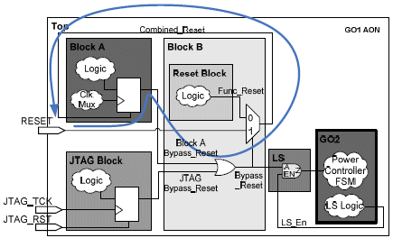
Fig. 6. Reset generation logic circuit.
Figure 6 shows the reset generation circuit of Block A which is in GO1_AON region. In test modes of the chip, it is required to bypass the reset such that it can be controlled through the main reset (RESET). Bypass_Reset signal is generated for this purpose from an output of an OR gate. One of the inputs of the OR gate is coming from a FF output which is actually inside Block A and the reset of this FF is the reset that is bypassed. This creates a loop which is undefined initially because reset generation circuit contains logic that is depending on the register output which is resetted by the reset itself. The arrow in the diagram shows this loop. As a result when GO1_AON region is powered, the reset of the FF stays undefined and all registers that are resetted by Combined_Reset signal can not be resetted properly.
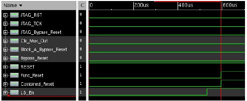
Fig. 7. Logic simulation without CPF.
However, during gate level simulations where CPF is not used as shown in Figure 7, the problem mentioned above can not be spotted because even though GO1_AON power region is shutoff from startup until around 400us, all the signals inside GO1_AON region is initialized successfully. This results in reset generation logic signal to be successfully defined as well.
Figure 8 shows the simulations with CPF. In real chip, this region has no power until 400us. As soon as the power is on in GO1_AON region at 400us, Block_A_Bypass_Reset signal becomes ‘X’ due to the reset dependency problem. This causes Combined_Reset signal, which is the reset of Block A to be ‘X’ causing all FFs’ outputs to be ‘X’ as well. The ‘X’s then propagate to entire design and the simulation fails.
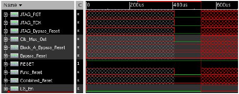
Fig. 8. Logic simulation with CPF.
Figure 9 shows the workaround that is used for the simulations to pass. Bypass_Reset signal is forced to logic ‘0’ from start up until some time after 400us. This results in Combined_Reset logic to be well defined and the simulation with CPF passes. Again, this is a workaround for CPF based simulations to pass and design needs to be modified to get rid of the loop back. In the new cut of the chip, the problem is solved with removing the dependency of Bypass_Reset signal to the FF inside Block A.
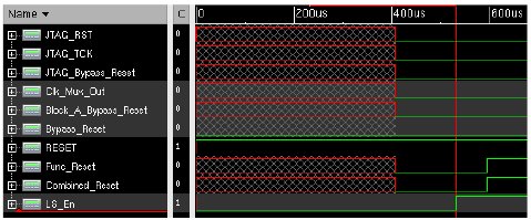
Fig. 9. Logic simulation with CPF and Bypass_Reset is forced.
VI. BUS MUXING LOGIC
This item, unlike the previous ones, points to the pessimism of CPF simulation flow through an example that has been faced during gate level simulations.
As seen in the Figure 10, an Interface Master Selection block exists in the design that also includes an Arbiter. Purpose of this blocks’ existence is to grant the control of the interface between two masters that are Block A and Block B. Interface Master Selection is a 3rd party module and has the capability of handling 256 masters, but for this design only two masters are controlling the interface.
Block A and Interface Master Selection Blocks are in GO1_SW region where Block B is in GO1_AON. The default control of the interface is granted to Block A. A mode named Sleep is defined for the chip that GO2 and GO1_AON are powered on where GO1_SW is powered off.
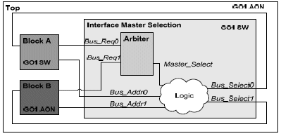
Fig. 10. Bus muxing logic.
Problem pops up when GO1_SW wakes up from the Sleep mode and last control of the interface is granted to Block B. The arbiter logic contains unresetable registers. The initialization of these registers is completed via several clock pulses. Going to sleep mode, the Master_Select output of the Arbiter goes to ‘X’ and keeps this value till the clock arrival. Even the GO1_SW is powered up the mentioned registers take ‘X’ value depending on the defined models of them. With the clock arrival the logic block propagates the ‘X’ value to Bus_Select* signals; ‘X’ propagation wins the race against the initialization of unresetable registers and breaks up the system.
The root of the problem is the unresetable registers that are still staying at ‘X’ value even the GO1_SW domain is powered on. In real life even though the register outputs are unknown they should either be ‘1’ or ‘0’. Depending on the behavioral model the simulator defines this unknown state as ‘X’. However, in this particular case having ‘0’ or ‘1’ at the output of the registers doesn’t have any difference in terms of functionality and the CPF simulation should have passed.
Figure 11 shows that without CPF the Master_Select bus keeps the value before power off. After initialization of unresetable registers, Interface Master Selection block is ready and provides the interface to the master depending on the request.

Fig. 11. Logic simulation without CPF.
Figure 12 shows that with CPF the Master_Select is ‘X’ before the first clock edge arrival, even if the Master_Select gets value ‘1’ with the clock arrival the ‘X’s are getting propagated to the Bus_Select* signals with the same clock and brakes up the system.
In theory, the initial value of Master_Select bus has no importance as the interface is granted to the requester master immediately depending on the priority order. To prove that on test bench a couple of simulation trials performed (please see Figures 12-15) by forcing the Master_Select signal after the wake up from Sleep and releasing the signal just after the clock arrival. It is proved that every time the interface is granted to the default master and once there is a request, the bus is granted to the requester master properly. As a result, the Master_Select signal taking ‘X’ value after GO1_SW domain is powered on is a too pessimistic behaviour that causes unnecessary debug time.

Fig. 12. Logic simulation with CPF.

Fig. 13. Logic Simulation with CPF and Master_Select is forced to ‘1’ that is the default value of Master_Select signal. Once clock has arrived the Master_Select signal is released & the signal keeps the value, after a couple of clock cycles a bus request popped from the other master & arbiter grants the bus to the requester.out

Fig. 14. Logic Simulation with CPF and Master_Select is forced to ‘2’. Once clock has arrived Master_Select signal is released & Arbiter granted the bus to the default master (0) (taking value ‘1’), soon a bus request popped from the other master & arbiter grants the bus to the requester.

Figure 15 - Logic Simulation with CPF and Master_Select is forced to 0XF. Once clock arrived the Master_Select signal is released & Arbiter granted the bus to the default master (0) (taking value ‘1’), soon a bus request popped from the other master & arbiter grants the bus to the requester.
VII. CONCLUSION
CPF is a very valuable verification methodology to verify the design on Low Power aspects in the early design stages. This paper presented three real SoC design examples to point out the importance of CPF based verification in low power designs. The first two examples clearly show that using a CPF based verification methodology would immediately reveal design problems that need to be fixed which could not otherwise be seen by other verification methodology that is not using CPF. On the other hand, third example points out to the pessimism of CPF based verification that the designers should also be aware of. In some cases, ‘X’ propagation by the simulator can cause the ‘X’s to propagate to all design causing simulations to fail where in parallel with the reality forcing the ‘X’ valued points with fixed values as it will be the case inside the real silicon will result in simulations to pass.
REFERENCES
[1] Atrenta Low Power Design Sub-Methodology, 2011.
[2] Atrenta SpyGlass Power Verify Rules Reference Guide, 2011.
[3] Si2 CPF 1.0 Tutorial, Dec. 2007., [Online] Available: http://www.si2.org/openeda.si2.org/cpf_tutorial_20071206/.
[4] Si2 Common Power Format Specification V1.0, V1.1,V2.0. [Online] Available: http://www.si2.org/openeda.si2.org/project/showfiles.php?group_id=51.
[5] Cadence CPF Methodology Guide, Version 1.0, 2010.
[6] Cadence Common Power Format Language Reference, Version 1.1, 2010.
[7] Cadence Common Power Format User Guide, Version 1.1, 2010. [8] Cadence Low-Power Verification Methodology, Version 8.2, 2009.
Related Semiconductor IP
- UFS 5.0 Host Controller IP
- PDM Receiver/PDM-to-PCM Converter
- Voltage and Temperature Sensor with integrated ADC - GlobalFoundries® 22FDX®
- 8MHz / 40MHz Pierce Oscillator - X-FAB XT018-0.18µm
- UCIe RX Interface
Related Articles
- Challenges and Benefits of Low Power Design Verification with CPF for a standalone IP
- Techniques for CDC Verification of an SoC
- Interconnect (NoC) verification in SoC design
- Shifting Mindsets: Static Verification Transforms SoC Design at RT Level
Latest Articles
- Enabling RISC-V Vector Code Generation in MLIR through Custom xDSL Lowerings
- A Scalable Open-Source QEC System with Sub-Microsecond Decoding-Feedback Latency
- SNAP-V: A RISC-V SoC with Configurable Neuromorphic Acceleration for Small-Scale Spiking Neural Networks
- An FPGA Implementation of Displacement Vector Search for Intra Pattern Copy in JPEG XS
- A Persistent-State Dataflow Accelerator for Memory-Bound Linear Attention Decode on FPGA