Breaking the 2 Giga Access Barrier: Overcoming Limited I/O Pin Counts
By Michael Miller, VP, Technology Innovation & Systems Applications MoSys, Inc.
Introduction :
Cisco’s Visual Networking Index forecasts that the Internet growth will quadruple by 2013. Projected Internet traffic will approach 1 Zettabyte (1 trillion Gigabytes) per year. To support this amazing trend, the next generations of networking equipment must offer new levels of packet forwarding rates and bandwidth density. This in turn will necessitate new generations of packet processors and the memory subsystems to support these increased demands. MoSys is stepping up to this challenge by introducing a new class of device to accelerate access to packet forwarding information, statistics calculations and packet storage.
Bandwidth intensive applications like video-on-demand, IPTV, P2P, Cloud Computing, 3G Wireless, VoIP and many others continue to spur this rapid expansion. Designers face the challenge of increasing the throughput of all subsystems for a variety of applications including video games, medical records, imaging transfers, and many more.

Figure 1: Graph of Projected Internet Growth
These increased demands strain communication between onboard devices, limiting the data throughput in network switches and routers. Like Moore’s Law, the amount of data throughput for network devices has doubled approximately every 18 months. Data transfer rates in optical devices are doubling even faster, every 9 months, as noted above.
To keep up, designers of network 10/40 Gbps Line Cards (also called Blades) must overcome the physical limitation
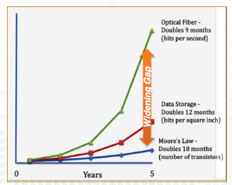
Figure 2: Projected 5-year Data Transfer Gap
of pin counts on their packet processing engine (ASIC, NPU, or FPGA). The question facing each developer is: How do I double, triple or quadruple the bandwidth density and number of accesses in the next generation?
Today, current limitations are usually thought of in terms of a trade-off between access speed and memory density, as embodied in SRAM vs. DRAM devices. To address these scaled-up throughput demands, we must abandon the traditional trade-offs.
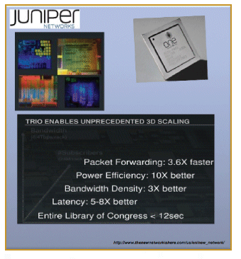
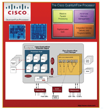
Juniper & Cisco Confirm Scaled Up Throughput
OEMs like Juniper Networks and Cisco Systems confirm these demanding next generation system requirements with new chipsets. Juniper’s recent releases boast impressive performance specs in packet forwarding, power efficiency and other key parameters noted in the graphic at the left 1.
On the right, 2 Cisco diagrams their QuantumFlow Processor (QFP) using their multi-flow packet architecture. Note the high number of memory chips surrounding the processor.
The Sea of Memory
To briefly review packet processing, a system with 100 Gbps throughput utilizes two different types of memory subsystems: The packet buffer in the Data Plane where packets are temporarily stored while they await forwarding and the table store in the Control Plane, which makes forwarding decisions. Currently these memory subsystems are constructed using DRAM and SRAM architectures, respectively. However, these designs are bumping up against limitations as designers implement 40G and 100G Ethernet blades. As a result, designs now sport ever-larger numbers of memory devices and the associated I/O connections to the packet processor, implemented in ASIC or FPGA.
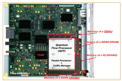
Figure 3: The Sea of Memory (Cisco ASR1000) 3
The Cisco ASR1000 (Shown above) typifies a 20 to 40 Gbps Ethernet line card performing Aggregation Service. Note the “Sea of Memory” surrounding the QFP. The board includes the following device counts: 4 - QDR (SRAM), 13 - DDRII (DRAM), 4 - RLDRAM (DRAM). In systems similar to this class of networking product, DDRII DRAM is often used for packet buffering because of the consumer PC pricing structure. RLDRAM is regularly used in the packet forwarding control path to implement forwarding decision trees. The QDR SRAM is a very low latency, high access rate memory that can be used for queue pointers and/or statistics.
To achieve 100 Gbps throughput on the packet processor, a typical system requires a temporary packet buffer with aggregate write/read throughput of 100 Gbps x 2 + 50% overhead, which approximates 300 Gbps. For the same 100 GB Ethernet application, the processor must be able to handle the minimum specified packet size of 64 bytes, which equates to an upper end rate of approximately 150 million packets per second.
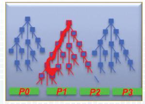
Figure 4: Representation of DecisionTree Path
The Control Plane, in conjunction with the packet processor, reads the header in the packet and directs it down the decision tree as represented in Fig. 4 above. Decisions include where to send the packet, what port to use, what priority, Yes-No decisions based on an Access Control List, Forward or Store, and more. This process requires conservatively 14 to 16 accesses. Higher speeds on the control plane memory reduce the number of parallel processes and therefore, fewer simultaneous threads of execution. Thus, fewer packets need to be stored in the packet buffer memory.
The 100 Gbps Ethernet Problem in Simple Math
ASICs and other packet processors cannot add any more I/O pins because they are at their physical limit of approximately 1,000 I/O pins. So let’s address accesses given the I/O limitation and available memory solutions. As noted above, buffer throughput must achieve approximately 300 Gbps and requires conservatively 12 to 13 next generation DDR3 memories. In turn, this requires approximately 300 pins of I/O on the processor.
To transmit 150 million packets per second requires a conservative average of 14 accesses per packet on the Control Plane, or 2.1 Giga Accesses per second. Next generation designs, as demonstrated on the Cisco line card above, require four RLDRAMII or QDR memories (since each operates at 533 million accesses per second). When implemented on the board, the Control Plane also requires 300 additional I/O pins at a minimum.
Thus, the packet processor requires at least 600-700 I/O pins (Control Plane + Buffer + misc. accesses) to communicate with the “sea of memory”. In current designs, devices communicate with other onboard devices by parallel transmission. However, since pin counts can no longer increase, it is hard to conceive of increasing bandwidth of a network processor beyond an aggregate throughput of 100 Gbps. To reach 200 to 400 Gbps, new kinds of memories and I/O must be considered. High-speed device-to-device serial communications provide the only pathway to a solution (see: Going Serial: Breaking the Billion Access Per Second Bandwidth Barrier).
Introducing Bandwidth Engine Technology
On February 2, 2010, MoSys introduced the new approach to breaking the Giga Accesses barrier, the Bandwidth Engine (BE) family of products. By implementing BE technology, designers can leverage an entirely new I/O paradigm. For a 100 Gbps throughput Ethernet design, BE chips specified on the Control Plane require only 64 I/0 pins vs. 300 for four RLDRAM, a 4-5 times reduction in pins. Applied on the buffer side, two BE’s require 128 pins (64 each) as versus 12 DDR III devices, which require approximately 300 pins, a 2-3 times reduction.
Comparing the combined control and buffer requirements for a 100 Gbps Ethernet line card, the BE solution requires 192 I/O pins as versus over 600 I/O pins using conventional approaches. Even RLDRAMII devices operating at 533 million accesses per second currently promise only 1 billion accesses in the next generation. BE technology delivers 2.5 Giga Accesses now.
Given market pricing pressures in the PC commodity market and significant density DRAM like DDR III, there will still be times when the designer chooses to use conventional DRAM for the packet buffer. But when bandwidth density is at a premium, the BE product family shines, even in the packet buffering memory subsystem. However, for control plane forward decision trees and statistics memory, there will be little choice. The BE family provides unparalleled performance and bandwidth density when compared to RLDRAM and QDR SRAM.
With significantly reduced I/O connections, designers can achieve new levels of bandwidth density. In advanced designs, they can tackle 2 to 4 times more network traffic on a single blade with a manageable number of ASICs.
Conclusion
Driven by a host of Internet applications, throughput requirements are rocketing upwards. However, the maximum I/O of current packet processors limits future performance objectives. At best, next generation Control Plane solutions promise to achieve only 1 billion accesses per second. MoSys’ BE devices signal a new paradigm, liberating designers by achieving up to 2.5 Giga Accesses per second, shrinking I/O pin requirements, and reducing board real estate.
Additional Reading & End Notes :
Going Serial: Breaking the Billion Access Per Second Bandwidth Barrier
1 Cisco Visual Networking Index. Source URL: https://www.cisco.com/en/US/netsol/ns827/networking_solutions_sub_solution.html - ~forecast
2 Juniper Networks. Source URL: http://www.thenewnetworkishere.com/us/en/new_network
3 Cisco Systems. Online source URL: http://www.cisco.com Written with the assistance of Lee Stein, Stein & Associates, Inc.
Related Semiconductor IP
- NPU IP Core for Mobile
- NPU IP Core for Edge
- Specialized Video Processing NPU IP
- HYPERBUS™ Memory Controller
- AV1 Video Encoder IP
Related White Papers
- Soc Design -> Soft design for cryptographic engine
- FPGAs: Embedded Apps : FPGA-based FFT engine handles four times more input data
- Royalty-free HyperTransport makes good on chip-to-chip bandwidth
- External Memory Interfaces: Delivering Bandwidth to Silicon
Latest White Papers
- Ramping Up Open-Source RISC-V Cores: Assessing the Energy Efficiency of Superscalar, Out-of-Order Execution
- Transition Fixes in 3nm Multi-Voltage SoC Design
- CXL Topology-Aware and Expander-Driven Prefetching: Unlocking SSD Performance
- Breaking the Memory Bandwidth Boundary. GDDR7 IP Design Challenges & Solutions
- Automating NoC Design to Tackle Rising SoC Complexity