Architecture and Implementation of the ARM Cortex-A8 Microprocessor
Introduction
The ARM® Cortex™-A8 microprocessor is the first applications microprocessor in ARM’s new Cortex family. With high performance and power efficiency, it targets a wide variety of mobile and consumer applications including mobile phones, set-top boxes, gaming consoles and automotive navigation/entertainment systems. The Cortex-A8 processor spans a range of performance points depending on the implementation, delivering over to 2000 Dhrystone MIPS (DMIPS) of performance for demanding consumer applications and consuming less than 300mW for low-power mobile devices. This translates into a large increase in processing capability while staying with the power levels of previous generations of mobile devices. Consumer applications will benefit from the reduced heat dissipation and resulting lower packaging and integration costs.
It is the first ARM processor to incorporate all of the new technologies available in the ARMv7 architecture. New technologies seen for the first time include NEON™ for media and signal processing and Jazelle® RCT for acceleration of realtime compilers. Other technologies recently introduced that are now standard on the ARMv7 architecture include TrustZone® technology for security, Thumb®-2 technology for code density and the VFPv3 floating point architecture.
Overview of the Cortex Architecture
The unifying technology of Cortex processors is Thumb-2 technology. The Thumb-2 instruction set combines 16- and 32-bit instructions to improve code density and performance. The original ARM instruction set consists of fixed-length 32-bit instructions, while the Thumb instruction set employs 16-bit instructions. Because not all operations mapped into the original Thumb instruction set, multiple instructions were sometimes needed to emulate the task of one 32-bit instruction.
Thumb-2 technology adds about 130 additional instructions to Thumb. The added functionality removes the need to switch between ARM and Thumb modes in order to service interrupts, and gives access to the full set of processor registers. The resulting code maintains the traditional code density of Thumb instructions while running at the performance levels of 32-bit ARM code. Entire applications can now be written in Thumb-2 technology, removing the original architecture required for mode switching.
An entire application can be written using space-saving Thumb-2 instructions, whereas with the original Thumb mode the processor had to switch between ARM and Thumb modes.
Making its first appearance in an ARM processor is the NEON media and signal processing technology targeted at audio, video and 3D graphics. It is a 64/128-bit hybrid SIMD architecture. NEON technology has its own register file and execution pipeline which are separate from the main ARM integer pipeline. It can handle both integer and single precision floating-point values, and includes support for unaligned data accesses and easy loading of interleaved data stored in structure form. Using NEON technology to perform typical multimedia functions, the Cortex-A8 processor can decode MPEG-4 VGA video (including dering, deblock filters and yuv2rgb) at 30 frames/sec at 275 MHz, and H.264 video at 350 MHz.
Also new is Jazelle RCT technology, an architecture extension that cuts the memory footprint of just-in-time (JIT) bytecode applications to a third of their original size. The smaller code size results in a boost performance and a reduction of power.
TrustZone technology is included in the Cortex-A8 to ensure data privacy and DRM protection in consumer products like mobile phones, personal digital assistants and set-top boxes that run open operating systems. Implemented within the processor core, TrustZone technology protects peripherals and memory against a security attack. A secure monitor within the core serves as a gatekeeper switching the system between secure and nonsecure states. In the secure state, the processor runs “trusted” code from a secure code block to handle security-sensitive tasks such as authentication and signature manipulation.
Besides contributing to the processor's signal processing performance, NEON technology enables software solutions to data processing applications. The result is a flexible platform which can accommodate new algorithms and new applications as they emerge with simply the download of new software or a driver.
The VFPv3 technology is an enhancement to the VFPv2 technology. New features include a doubling of the number of double-precision registers to 32, and the introduction of instructions that perform conversions between fixed-point and floating-point numbers.
Exploring Features of the Cortex-A8 Microarchitecture
The Cortex-A8 processor is the most sophisticated low-power design yet produced by ARM. To achieve its high levels of performance, new microarchitecture features were added which are not traditionally found in the ARM architecture, including a dual in-order issue ARM integer pipeline, an integrated L2 cache and a deep 13-stage pipe.
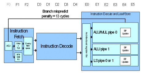
Superscalar Pipeline
Perhaps the most significant of these new features is the dual-issue, in-order, statically scheduled ARM integer pipeline. Previous ARM processors have only a single integer execution pipeline. The ability to issue two data processing instructions at the same time significantly increases the maximum potential instructions executed per cycle. It was decided to stay with in-order issue to keep additional power required to a minimum. Out-of-order issue and retire can require extensive amounts of logic consuming extra power. The choice to go with in-order also allows for fire-and-forget instruction issue, thus removing critical paths from the design and reducing the need for custom design in the pipeline. Static scheduling allows for extensive clock gating for reduced power during execution.
The dual ALU (arithmetic logic unit) pipelines (ALU 0 and ALU 1) are symmetric and both can handle most arithmetic instructions. ALU pipe 0 always carries the older of a pair of issued instructions. The Cortex-A8 processor also has multiplier and load-store pipelines, but these do not carry additional instructions to the two ALU pipelines. These can be thought of as “dependent” pipelines. Their use requires simultaneous use of one of the ALU pipelines. The multiplier pipeline can only be coupled with instructions that are in ALU 0 pipeline, whereas the load-store pipeline can be coupled with instructions in either ALU.
Branch Prediction
The 13-stage pipeline was selected to enable significantly higher operating frequencies than precious generations of ARM microarchitectures. Note that stage F0 is not counted because it is only address generation. To minimize the branch penalties typically associated with a deeper pipeline, the Cortex-A8 processor implements a two-level global history branch predictor. It consists of two different structures: the Branch Target Buffer (BTB) and the Global History Buffer (GHB) which are accessed in parallel with instruction fetches.
The BTB indicates whether or not the current fetch address will return a branch instruction and its branch target address. It contains 512 entries. On a hit in the BTB a branch is predicted and the GHB is accessed. The GHB consists of 4096 2-bit saturating counters that encode the strength and direction information of branches. The GHB is indexed by 10-bit history of the direction of the last ten branches encountered and 4 bits of the PC.
In addition to the dynamic branch predictor, a return stack is used to predict subroutine return addresses. The return stack has eight 32-bit entries that store the link register value in r14 (register 14) and the ARM or Thumb state of the calling function. When a return-type instruction is predicted taken, the return stack provides the last pushed address and state.
Level-1 Cache
The Cortex-A8 processor has a single-cycle load-use penalty for fast access to the Level-1 caches. The data and instruction caches are configurable to 16k or 32k. Each is 4-way set associative and uses a Hash Virtual Address Buffer (HVAB) way prediction scheme to improve timing and reduce power consumption. The caches are physically addressed (virtual index, physical tag) and have hardware support for avoiding aliased entries. Parity is supported with one parity bit per byte.
The replacement policy for the data cache is write-back with no write allocates. Also included is a store buffer for data merging before writing to main memory.
The HVAB is a novel approach to reducing the power required for accessing the caches. It uses a prediction scheme to determine which way of the RAM to enable before an access.
Level-2 Cache
The Cortex-A8 processor includes an integrated Level-2 cache. This gives the Level-2 cache a dedicated low latency, high bandwidth interface to the Level-l cache. This minimizes the latency of Level-1 cache linefills and does not conflict with traffic on the main system bus. It can be configured in sizes from 64k to 2M.
The Level-2 cache is physically addressed and 8-way set associative. It is a unified data and instruction cache, and supports optional ECC and Parity. Write back, write through, and write-allocate policies are followed according to page table settings. A pseudo-random allocation policy is used. The contents of the Level-1 data cache are exclusive with the Level-2 cache, whereas the contents of the Level-1 instruction cache are a subset of the Level-2 cache. The tag and data RAMs of the Level-2 cache are accessed serially for power savings.
NEON media engine
The Cortex-A8 processor’s NEON media processing engine pipeline starts at the end of the main integer pipeline. As a result, all exceptions and branch mispredictions are resolved before instructions reach it. More importantly, there is a zero load-use penalty for data in the Level-1 cache. The ARM integer unit generates the addresses for NEON loads and stores as they pass through the pipeline, thus allowing data to be fetched from the Level-1 cache before it is required by a NEON data processing operation. Deep instruction and load-data buffering between the NEON engine, the ARM integer unit and the memory system allow the latency of Level-2 accesses to be hidden for streamed data. A store buffer prevents NEON stores from blocking the pipeline and detects address collisions with the ARM integer unit accesses and NEON loads.
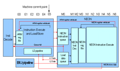
The NEON unit is decoupled from the main ARM integer pipeline by the NEON instruction queue (NIQ). The ARM Instruction Execute Unit can issue up to two valid instructions to the NEON unit each clock cycle. NEON has 128-bit wide load and store paths to the Level-1 and Level-2 cache, and supports streaming from both.
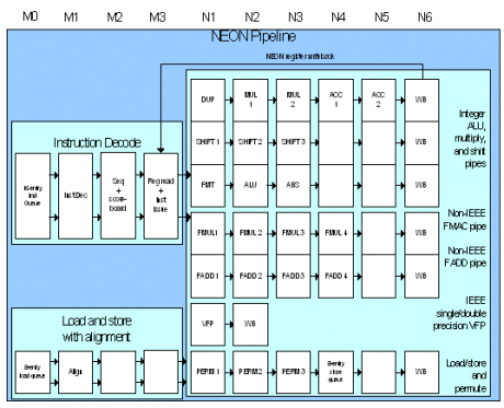
The NEON media engine has its own 10 stage pipeline that begins at the end ARM integer pipeline. Since all mispredicts and exceptions have been resolved in the ARM integer unit, once an instruction has been issued to the NEON media engine it must be completed as it cannot generate exceptions. NEON has three SIMD integer pipelines, a load-store/permute pipeline, two SIMD single-precision floating-point pipelines, and a non-pipelined Vector Floating-Point unit (VFPLite).
NEON instructions are issued and retired in-order. A data processing instruction is either a NEON integer instruction or a NEON floating-point instruction. The Cortex-A8 NEON unit does not parallel issue two data-processing instructions to avoid the area overhead with duplicating the data-processing functional blocks, and to avoid timing critical paths and complexity overhead associated with the muxing of the read and write register ports.
The NEON integer datapath consists of three pipelines: an integer multiply/accumulate pipeline (MAC), an integer Shift pipeline, and an integer ALU pipeline. A load-store/permute pipeline is responsible for all NEON load/stores, data transfers to/from the integer unit, and data permute operations such as interleave and de-interleave. The NEON floating-point (NFP) datapath has two main pipelines: a multiply pipeline and an add pipeline. The separate VFPLite unit is a non-pipelined implementation of the ARM
VFPv3 Floating Point Specification targeted for medium performance IEEE 754 compliant floating point support. VFPLite is used to provide backwards compatibility with existing ARM floating point code and to provide IEEE 754 compliant single and double precision arithmetic. The “Lite” refers to area and performance, not functionality.
Implementation
Because of the aggressive performance, power, and area targets (PPA) of the Cortex-A8 processor, new implementation flows have been developed in order to meet goals without resorting to a full-custom implementation. The resulting flows enable fine tuning of the design to the desired application. The result is fundamentally a cell-based flow, but under it lies semi-custom techniques that have been used where necessary to meet performance.
The Cortex-A8 processor uses a combination of synthesized, structured, and custom circuits. The design was divided into seven functional units and then subdivided into blocks, and the appropriate implementation technique chosen for each. Since the entire design is synthesizeable, blocks that can easily meet their PPA goals can stick with a standard synthesis flow.
A structured flow is used for blocks which contain logic that can take advantage of controlled placement and routing approach to meet timing or area goals. This approach is a semi-custom flow that manually maps the block into a gate-level netlist and specifies a relative placement for all the cells in the block. The relative placement does not specify the exact locations of the cells but how each cell is placed with respect to the other cells in the block.
The structured approach is typically used for data blocks that have regular structure. The logic implementation and technology mapping of the block is done manually to maintain the regular data-oriented bus structure of the block instead of generating a random gate structure through synthesis. The logic gates of the block are placed according to the flow of data through the block. This approach offers more control over the design than an automated synthesis approach and leads to a more predictable timing closure. It is also possible to get better performance and area on complex, high-performance designs than traditional techniques. The resulting netlists may be interpreted with traditional tiling techniques using the ARM Artisan® Advantage-CE™ or compatible library.
The Artisan Advantage-CE library contains more than a thousand cells. Besides the standard cells used typical synthesis libraries, many tactical cells are included more in line with custom implementation techniques. These are used in an automated fashion in the structured flow. The library is specifically designed to deal with the high-density routing requirements of high-performance processors with a focus on both high speed operation and low static and dynamic power. Leakage reduction is achieved through power gating MT-CMOS cells and retention flip-fops to support sleep and standby modes. ARM has worked with tool vendors to ensure support for this critical new flow.
Finally, a few of the most critical timing and area sensitive blocks of the design are reserved for full custom techniques. This includes memory arrays, register files and scoreboards. These blocks contain a mix of static and dynamic logic. No self-timed circuits are used.
Conclusion
The Cortex-A8 processor is the fastest, most power-efficient microprocessor yet developed by ARM. With the ability to decode VGA H.264 video in under 350MHz, it provides the media processing power required for next generation wireless and consumer products while consuming less than 300mW in 65nm technologies. Its new NEON technology provides a platform for flexible software-based solutions for media processing. Thumb-2 instructions provide code density while maintaining the performance of standard ARM code; Jazelle RCT technology does likewise for realtime compilers. TrustZone technology provides security for sensitive data and DRM.
Many significant new microarchitecture features make their first appearance on the Cortex-A8 processor. These include a dual issue, in-order superscalar pipeline, an integrated Level-2 cache and a significantly deeper pipeline than precious ARM processors. To meet its aggressive performance targets while maintaining ARM’s traditional small power budget, new flows have been developed which approach the efficiency of custom techniques while keeping the flexibility of an automated flow. The Cortex-A8 processor is a quantum jump in flexible low power, high-performance processing.
Footnote:
ARM’s new processor naming convention
With the announcement of the Cortex™-M3 processor, ARM introduced a new naming scheme for its processors. Previously processors were named for the base processor core such as ARM7™, ARM9™ and ARM11™, and digits were added to designate the features of that variation of the processor. Thus an ARM926EJ-S™ was based on the ARM9 microarchitecture, and digits were added to designate the memory system, Java support and arithmetic extensions.
The new ARM naming scheme is based on the generation of architecture of the processor, and not sequence of arrival of the processor itself. (At ARM an architecture refers to an instruction/feature set common to a group of processors.) Cores which belong to the latest generation of ARM architecture, ARMv7, will all be know as “Cortex” processors. The next generation of processors will be given yet another new name. This was done to give a clearer understanding of the relative performance and target application of a new processor from its name.
The ARMv7 architecture and thus the Cortex processors will be divided into three main groups: Applications (A) processors, Realtime (R) processors and Microcontrollors (M). Applications processors are intended for use with open OS and feature a memory
management unit (MMU) providing for virtual addressing. Realtime processors will focus more deeply embedded applications. They will feature a memory protection unit (MPU) which protects regions of memory but does not provide for virtual addressing. Microcontrollers will generally not have memory protection, and focus on providing very low latency responses to interrupts and including features such as flash memory controllers and interrupt controllers. The group to which a processor belongs is designated by adding a -A, -R or -M to the base Cortex name.
The ARM® Cortex™-A8 microprocessor is the first applications microprocessor in ARM’s new Cortex family. With high performance and power efficiency, it targets a wide variety of mobile and consumer applications including mobile phones, set-top boxes, gaming consoles and automotive navigation/entertainment systems. The Cortex-A8 processor spans a range of performance points depending on the implementation, delivering over to 2000 Dhrystone MIPS (DMIPS) of performance for demanding consumer applications and consuming less than 300mW for low-power mobile devices. This translates into a large increase in processing capability while staying with the power levels of previous generations of mobile devices. Consumer applications will benefit from the reduced heat dissipation and resulting lower packaging and integration costs.
It is the first ARM processor to incorporate all of the new technologies available in the ARMv7 architecture. New technologies seen for the first time include NEON™ for media and signal processing and Jazelle® RCT for acceleration of realtime compilers. Other technologies recently introduced that are now standard on the ARMv7 architecture include TrustZone® technology for security, Thumb®-2 technology for code density and the VFPv3 floating point architecture.
Overview of the Cortex Architecture
The unifying technology of Cortex processors is Thumb-2 technology. The Thumb-2 instruction set combines 16- and 32-bit instructions to improve code density and performance. The original ARM instruction set consists of fixed-length 32-bit instructions, while the Thumb instruction set employs 16-bit instructions. Because not all operations mapped into the original Thumb instruction set, multiple instructions were sometimes needed to emulate the task of one 32-bit instruction.
Thumb-2 technology adds about 130 additional instructions to Thumb. The added functionality removes the need to switch between ARM and Thumb modes in order to service interrupts, and gives access to the full set of processor registers. The resulting code maintains the traditional code density of Thumb instructions while running at the performance levels of 32-bit ARM code. Entire applications can now be written in Thumb-2 technology, removing the original architecture required for mode switching.
An entire application can be written using space-saving Thumb-2 instructions, whereas with the original Thumb mode the processor had to switch between ARM and Thumb modes.
Making its first appearance in an ARM processor is the NEON media and signal processing technology targeted at audio, video and 3D graphics. It is a 64/128-bit hybrid SIMD architecture. NEON technology has its own register file and execution pipeline which are separate from the main ARM integer pipeline. It can handle both integer and single precision floating-point values, and includes support for unaligned data accesses and easy loading of interleaved data stored in structure form. Using NEON technology to perform typical multimedia functions, the Cortex-A8 processor can decode MPEG-4 VGA video (including dering, deblock filters and yuv2rgb) at 30 frames/sec at 275 MHz, and H.264 video at 350 MHz.
Also new is Jazelle RCT technology, an architecture extension that cuts the memory footprint of just-in-time (JIT) bytecode applications to a third of their original size. The smaller code size results in a boost performance and a reduction of power.
TrustZone technology is included in the Cortex-A8 to ensure data privacy and DRM protection in consumer products like mobile phones, personal digital assistants and set-top boxes that run open operating systems. Implemented within the processor core, TrustZone technology protects peripherals and memory against a security attack. A secure monitor within the core serves as a gatekeeper switching the system between secure and nonsecure states. In the secure state, the processor runs “trusted” code from a secure code block to handle security-sensitive tasks such as authentication and signature manipulation.
Besides contributing to the processor's signal processing performance, NEON technology enables software solutions to data processing applications. The result is a flexible platform which can accommodate new algorithms and new applications as they emerge with simply the download of new software or a driver.
The VFPv3 technology is an enhancement to the VFPv2 technology. New features include a doubling of the number of double-precision registers to 32, and the introduction of instructions that perform conversions between fixed-point and floating-point numbers.
Exploring Features of the Cortex-A8 Microarchitecture
The Cortex-A8 processor is the most sophisticated low-power design yet produced by ARM. To achieve its high levels of performance, new microarchitecture features were added which are not traditionally found in the ARM architecture, including a dual in-order issue ARM integer pipeline, an integrated L2 cache and a deep 13-stage pipe.

Superscalar Pipeline
Perhaps the most significant of these new features is the dual-issue, in-order, statically scheduled ARM integer pipeline. Previous ARM processors have only a single integer execution pipeline. The ability to issue two data processing instructions at the same time significantly increases the maximum potential instructions executed per cycle. It was decided to stay with in-order issue to keep additional power required to a minimum. Out-of-order issue and retire can require extensive amounts of logic consuming extra power. The choice to go with in-order also allows for fire-and-forget instruction issue, thus removing critical paths from the design and reducing the need for custom design in the pipeline. Static scheduling allows for extensive clock gating for reduced power during execution.
The dual ALU (arithmetic logic unit) pipelines (ALU 0 and ALU 1) are symmetric and both can handle most arithmetic instructions. ALU pipe 0 always carries the older of a pair of issued instructions. The Cortex-A8 processor also has multiplier and load-store pipelines, but these do not carry additional instructions to the two ALU pipelines. These can be thought of as “dependent” pipelines. Their use requires simultaneous use of one of the ALU pipelines. The multiplier pipeline can only be coupled with instructions that are in ALU 0 pipeline, whereas the load-store pipeline can be coupled with instructions in either ALU.
Branch Prediction
The 13-stage pipeline was selected to enable significantly higher operating frequencies than precious generations of ARM microarchitectures. Note that stage F0 is not counted because it is only address generation. To minimize the branch penalties typically associated with a deeper pipeline, the Cortex-A8 processor implements a two-level global history branch predictor. It consists of two different structures: the Branch Target Buffer (BTB) and the Global History Buffer (GHB) which are accessed in parallel with instruction fetches.
The BTB indicates whether or not the current fetch address will return a branch instruction and its branch target address. It contains 512 entries. On a hit in the BTB a branch is predicted and the GHB is accessed. The GHB consists of 4096 2-bit saturating counters that encode the strength and direction information of branches. The GHB is indexed by 10-bit history of the direction of the last ten branches encountered and 4 bits of the PC.
In addition to the dynamic branch predictor, a return stack is used to predict subroutine return addresses. The return stack has eight 32-bit entries that store the link register value in r14 (register 14) and the ARM or Thumb state of the calling function. When a return-type instruction is predicted taken, the return stack provides the last pushed address and state.
Level-1 Cache
The Cortex-A8 processor has a single-cycle load-use penalty for fast access to the Level-1 caches. The data and instruction caches are configurable to 16k or 32k. Each is 4-way set associative and uses a Hash Virtual Address Buffer (HVAB) way prediction scheme to improve timing and reduce power consumption. The caches are physically addressed (virtual index, physical tag) and have hardware support for avoiding aliased entries. Parity is supported with one parity bit per byte.
The replacement policy for the data cache is write-back with no write allocates. Also included is a store buffer for data merging before writing to main memory.
The HVAB is a novel approach to reducing the power required for accessing the caches. It uses a prediction scheme to determine which way of the RAM to enable before an access.
Level-2 Cache
The Cortex-A8 processor includes an integrated Level-2 cache. This gives the Level-2 cache a dedicated low latency, high bandwidth interface to the Level-l cache. This minimizes the latency of Level-1 cache linefills and does not conflict with traffic on the main system bus. It can be configured in sizes from 64k to 2M.
The Level-2 cache is physically addressed and 8-way set associative. It is a unified data and instruction cache, and supports optional ECC and Parity. Write back, write through, and write-allocate policies are followed according to page table settings. A pseudo-random allocation policy is used. The contents of the Level-1 data cache are exclusive with the Level-2 cache, whereas the contents of the Level-1 instruction cache are a subset of the Level-2 cache. The tag and data RAMs of the Level-2 cache are accessed serially for power savings.
NEON media engine
The Cortex-A8 processor’s NEON media processing engine pipeline starts at the end of the main integer pipeline. As a result, all exceptions and branch mispredictions are resolved before instructions reach it. More importantly, there is a zero load-use penalty for data in the Level-1 cache. The ARM integer unit generates the addresses for NEON loads and stores as they pass through the pipeline, thus allowing data to be fetched from the Level-1 cache before it is required by a NEON data processing operation. Deep instruction and load-data buffering between the NEON engine, the ARM integer unit and the memory system allow the latency of Level-2 accesses to be hidden for streamed data. A store buffer prevents NEON stores from blocking the pipeline and detects address collisions with the ARM integer unit accesses and NEON loads.

The NEON unit is decoupled from the main ARM integer pipeline by the NEON instruction queue (NIQ). The ARM Instruction Execute Unit can issue up to two valid instructions to the NEON unit each clock cycle. NEON has 128-bit wide load and store paths to the Level-1 and Level-2 cache, and supports streaming from both.
The NEON media engine has its own 10 stage pipeline that begins at the end ARM integer pipeline. Since all mispredicts and exceptions have been resolved in the ARM integer unit, once an instruction has been issued to the NEON media engine it must be completed as it cannot generate exceptions. NEON has three SIMD integer pipelines, a load-store/permute pipeline, two SIMD single-precision floating-point pipelines, and a non-pipelined Vector Floating-Point unit (VFPLite).
NEON instructions are issued and retired in-order. A data processing instruction is either a NEON integer instruction or a NEON floating-point instruction. The Cortex-A8 NEON unit does not parallel issue two data-processing instructions to avoid the area overhead with duplicating the data-processing functional blocks, and to avoid timing critical paths and complexity overhead associated with the muxing of the read and write register ports.
The NEON integer datapath consists of three pipelines: an integer multiply/accumulate pipeline (MAC), an integer Shift pipeline, and an integer ALU pipeline. A load-store/permute pipeline is responsible for all NEON load/stores, data transfers to/from the integer unit, and data permute operations such as interleave and de-interleave. The NEON floating-point (NFP) datapath has two main pipelines: a multiply pipeline and an add pipeline. The separate VFPLite unit is a non-pipelined implementation of the ARM
VFPv3 Floating Point Specification targeted for medium performance IEEE 754 compliant floating point support. VFPLite is used to provide backwards compatibility with existing ARM floating point code and to provide IEEE 754 compliant single and double precision arithmetic. The “Lite” refers to area and performance, not functionality.

Implementation
Because of the aggressive performance, power, and area targets (PPA) of the Cortex-A8 processor, new implementation flows have been developed in order to meet goals without resorting to a full-custom implementation. The resulting flows enable fine tuning of the design to the desired application. The result is fundamentally a cell-based flow, but under it lies semi-custom techniques that have been used where necessary to meet performance.
The Cortex-A8 processor uses a combination of synthesized, structured, and custom circuits. The design was divided into seven functional units and then subdivided into blocks, and the appropriate implementation technique chosen for each. Since the entire design is synthesizeable, blocks that can easily meet their PPA goals can stick with a standard synthesis flow.
A structured flow is used for blocks which contain logic that can take advantage of controlled placement and routing approach to meet timing or area goals. This approach is a semi-custom flow that manually maps the block into a gate-level netlist and specifies a relative placement for all the cells in the block. The relative placement does not specify the exact locations of the cells but how each cell is placed with respect to the other cells in the block.
The structured approach is typically used for data blocks that have regular structure. The logic implementation and technology mapping of the block is done manually to maintain the regular data-oriented bus structure of the block instead of generating a random gate structure through synthesis. The logic gates of the block are placed according to the flow of data through the block. This approach offers more control over the design than an automated synthesis approach and leads to a more predictable timing closure. It is also possible to get better performance and area on complex, high-performance designs than traditional techniques. The resulting netlists may be interpreted with traditional tiling techniques using the ARM Artisan® Advantage-CE™ or compatible library.
The Artisan Advantage-CE library contains more than a thousand cells. Besides the standard cells used typical synthesis libraries, many tactical cells are included more in line with custom implementation techniques. These are used in an automated fashion in the structured flow. The library is specifically designed to deal with the high-density routing requirements of high-performance processors with a focus on both high speed operation and low static and dynamic power. Leakage reduction is achieved through power gating MT-CMOS cells and retention flip-fops to support sleep and standby modes. ARM has worked with tool vendors to ensure support for this critical new flow.
Finally, a few of the most critical timing and area sensitive blocks of the design are reserved for full custom techniques. This includes memory arrays, register files and scoreboards. These blocks contain a mix of static and dynamic logic. No self-timed circuits are used.
Conclusion
The Cortex-A8 processor is the fastest, most power-efficient microprocessor yet developed by ARM. With the ability to decode VGA H.264 video in under 350MHz, it provides the media processing power required for next generation wireless and consumer products while consuming less than 300mW in 65nm technologies. Its new NEON technology provides a platform for flexible software-based solutions for media processing. Thumb-2 instructions provide code density while maintaining the performance of standard ARM code; Jazelle RCT technology does likewise for realtime compilers. TrustZone technology provides security for sensitive data and DRM.
Many significant new microarchitecture features make their first appearance on the Cortex-A8 processor. These include a dual issue, in-order superscalar pipeline, an integrated Level-2 cache and a significantly deeper pipeline than precious ARM processors. To meet its aggressive performance targets while maintaining ARM’s traditional small power budget, new flows have been developed which approach the efficiency of custom techniques while keeping the flexibility of an automated flow. The Cortex-A8 processor is a quantum jump in flexible low power, high-performance processing.
Footnote:
ARM’s new processor naming convention
With the announcement of the Cortex™-M3 processor, ARM introduced a new naming scheme for its processors. Previously processors were named for the base processor core such as ARM7™, ARM9™ and ARM11™, and digits were added to designate the features of that variation of the processor. Thus an ARM926EJ-S™ was based on the ARM9 microarchitecture, and digits were added to designate the memory system, Java support and arithmetic extensions.
The new ARM naming scheme is based on the generation of architecture of the processor, and not sequence of arrival of the processor itself. (At ARM an architecture refers to an instruction/feature set common to a group of processors.) Cores which belong to the latest generation of ARM architecture, ARMv7, will all be know as “Cortex” processors. The next generation of processors will be given yet another new name. This was done to give a clearer understanding of the relative performance and target application of a new processor from its name.
The ARMv7 architecture and thus the Cortex processors will be divided into three main groups: Applications (A) processors, Realtime (R) processors and Microcontrollors (M). Applications processors are intended for use with open OS and feature a memory
management unit (MMU) providing for virtual addressing. Realtime processors will focus more deeply embedded applications. They will feature a memory protection unit (MPU) which protects regions of memory but does not provide for virtual addressing. Microcontrollers will generally not have memory protection, and focus on providing very low latency responses to interrupts and including features such as flash memory controllers and interrupt controllers. The group to which a processor belongs is designated by adding a -A, -R or -M to the base Cortex name.
Related Semiconductor IP
- 6809 compatible 8-bit microprocessor
- Microprocessor IP for video codecs and video processing -- High Number of Streams Decoder For Data Center
- Microprocessor IP for video codecs and video processing -- High Number of Streams Encoder For Data Center
- 8-Bit Microprocessor Core
- 8-bit Microprocessor
Related Articles
- Why Embedded Software Development Still Matters: Optimizing a Computer Vision Application on the ARM Cortex A8
- An 800 Mpixels/s, ~260 LUTs Implementation of the QOI Lossless Image Compression Algorithm and its Improvement through Hilbert Scanning
- M31 on the Specification and Development of MIPI Physical Layer
- The Future of Safe and Secure Aerospace Systems
Latest Articles
- Extending and Accelerating Inner Product Masking with Fault Detection via Instruction Set Extension
- ioPUF+: A PUF Based on I/O Pull-Up/Down Resistors for Secret Key Generation in IoT Nodes
- In-Situ Encryption of Single-Transistor Nonvolatile Memories without Density Loss
- David vs. Goliath: Can Small Models Win Big with Agentic AI in Hardware Design?
- RoMe: Row Granularity Access Memory System for Large Language Models