Analyzing Modern NVIDIA GPU cores
By Rodrigo Huerta, Mojtaba Abaie Shoushtary, José-Lorenzo Cruz and Antonio González, Universitat Politècnica de Catalunya, Barcelona, Spain
Abstract
GPUs are the most popular platform for accelerating HPC work-loads, such as artificial intelligence and science simulations. How-ever, most microarchitectural research in academia relies on GPU core pipeline designs based on architectures that are more than 15 years old.
This paper reverse engineers modern NVIDIA GPU cores, unveiling many key aspects of its design and explaining how GPUs leverage hardware-compiler techniques where the compiler guides hardware during execution. In particular, it reveals how the issue logic works including the policy of the issue scheduler, the structure of the register file and its associated cache, and multiple features of the memory pipeline. Moreover, it analyses how a simple instruction prefetcher based on a stream buffer fits well with modern NVIDIA GPUs and is likely to be used. Furthermore, we investigate the impact of the register file cache and the number of register file read ports on both simulation accuracy and performance.
By modeling all these new discovered microarchitectural details, we achieve 18.24% lower mean absolute percentage error (MAPE) inexecutioncyclesthanpreviousstate-of-the-artsimulators,result-ing in an average of 13.98% MAPE with respect to real hardware (NVIDIA RTX A6000). Also, we demonstrate that this new model stands for other NVIDIA architectures, such as Turing.
Finally, we show that the software-based dependence management mechanism included in modern NVIDIA GPUs outperforms a hardware mechanism based on score boards in terms of performance and area.
1. Introduction
In recent years, GPUs have become very popular for executing general-purpose workloads [21] in addition to graphics. GPUs’ architecture provides massive parallelism that can be leveraged by many modern applications such as bio informatics[23,59],physics[52, 87], and chemistry [39, 89], to name a few. Nowadays, GPUs are the main candidates to accelerate modern machine learning work-loads, which have high memory bandwidth and computation demands [27]. Over the last years, there have been significant innovations in GPUs’ microarchitecture, their interconnection technolo-gies(NVLink[63]),andtheircommunicationframeworks(NCCL[64]). All these advances have enabled inference and training of Large Language Models, which require clusters with thousands of GPUs [56].
However, there is scarce information on the microarchitecture design of modern commercial GPUs, and current academic studies [17, 49] take the Tesla microarchitecture [51] as the baseline, which was launched in 2006. Today GPU architectures has under-gone significant changes since Tesla, hence, a model based on that can deviate the reported findings. This work aims to unveil different features and details of various components that modern NVIDIA GPU architectures use to improve the accuracy of academic microarchitecture models. The model and details explained in this work allow researchers to better identify challenges and opportunities for improving future GPUs. In summary, this paper makes the following contributions:
- Describes the operation of the issue stage, including dependence handling, readiness conditions of warps, and the issue scheduler policy.
- Describes a plausible operation of the fetch stage and its scheduler that coordinates with the issue stage.
- Provides important details of the register file and explains the behavior of the register file cache. Moreover, it shows that modern NVIDIA GPUs do not use an operand collection stage or collector units.
- Reveals multiple details of the components of the memory pipeline.
- Redesigns the SM/core model used in Accel-sim simulator [49] from scratch and integrates all the details we revealed in this paper into the model.
- Validates the new model against real hardware and com-pares it against the Accel-sim simulator [49]. Our new model achieves a mean absolute percentage error (MAPE) of execution cycles against real hardware of 13.98% for the NVIDIA RTX A6000 (Ampere), which is 18.24% better than the previous simulator model.
- Demonstrates that a naive stream buffer for instruction prefetching provides a greater performance accuracy, and its performance is similar to a perfect instruction cache.
- Shows how the register file cache and the number of register file read ports affect simulation accuracy and performance.
- Compares the performance, area, and simulation accuracy of the dependence management system that we unveil in this paper against the traditional scoreboard. The comparison reveals that this novel software-hardware co-design is a more efficient alternative than handling dependencies with traditional scoreboards.
- Shows the portability of the model to other NVIDIA architectures such as Turing.
The rest of this paper is organized as follows. First, we introduce the background and motivation of this work in section 2. In section 3, we explain the reverse engineering methodology that we have employed. We describe the control bits in modern NVIDIA GPU architectures and their detailed behavior in section 4. Later, we present the core microarchitecture of these GPUs in section 5.
Next, we describe the features we have modeled in our simulator in section6.Section7evaluatestheaccuracyofourmodelagainstreal hardware and compares it to the Accel-sim framework simulator, analyzes the impact of a stream buffer for instruction prefetch-ing, studies the effect of the register file cache and the number of register file read ports, compares different dependence management mechanisms, and discusses how the model stands for other NVIDIA architectures. Section 8 reviews previous related work. Finally, section 9 summarizes the main lessons of this work.
2. Background and Motivation
Most GPU microarchitecture research in academia relies on the microarchitecture that GPGPU-Sim simulator employs [1, 17]. Recently, this simulator was updated to include sub-cores (Processing Blocks in NVIDIA terminology) approach that started in Volta. Figure 1 shows a block diagram of the architecture modeled in this simulator. We can observe that it comprises four sub-cores and some shared components, such as the L1 instruction cache, L1 data cache, shared memory, and texture units.
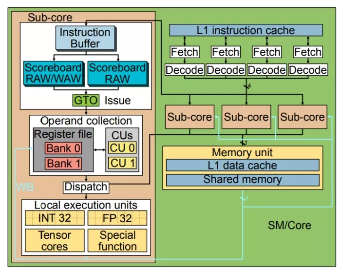
Figure 1: SM/Core academia design.
In the Fetch stage of this GPU pipeline, a round robin scheduler selects a warp whose next instruction is in the L1 instruction cache and has empty slots in the Instruction Buffers. These buffers are dedicated per warp and store the consecutive instructions of a warp after they are fetched and decoded. Instructions stay in this buffer until they are ready and selected to be issued.
In the Issue stage, a Greedy Then Oldest (GTO) [77] scheduler selects a warp if it is not waiting on a barrier and its oldest instruction does not have data dependence with other in-flight instructions in the pipeline. Previous works assume that each warp has two scoreboards for checking the data dependence. The first one marks pending writes to the registers to track WAW and RAW dependencies. An instruction can be issued only when all its operands are cleared in this scoreboard. The second scoreboard counts the number of in-flight consumers of registers to prevent WAR hazards [57]. The second scoreboard is necessary because although instructions are issued in-order, their operands might be fetched out of order. This happens for variable-latency instructions such as memory instructions. These instructions are queued after being issued and may read its source operands after a younger arithmetic instruction writes its result, causing a WAR hazard if the source operand of the former is the same as the destination operand of the latter.
Once an instruction is issued, it is placed in a Collector Unit (CU) and waits until all its source register operands are retrieved. Each sub-core has a private register file with multiple banks and a few ports per bank, allowing for multiple accesses in a single cycle at a low cost. An arbiter deals with the possible conflicts among several petitions to the same bank. When all source operands of an instruction are in the CU, the instruction moves to the Dispatch stage, where it is dispatched to the proper execution unit (e.g., memory, single-precision, special function) whose latencies differ depending on the unit type and instruction. Once the instruction reaches the write-back stage, the result is written in the register file.
This GPU microarchitecture modeled in Accel-sim [49] resembles NVIDIA GPUs based on Tesla [51], which was released in 2006, and updated with a few modern features, mainly a sub-core model and sectored caches with IPOLY [75] indexing similar to Volta [49]. However, it lacks some important components that are present in modern NVIDIA GPUs, such as the L0 instruction cache [20, 28, 65– 69] and the uniform register file [20]. Moreover, some main components of sub-cores, such as the issue logic, register file, or register file caches, among others, are not updated to reflect current designs.
This work aims to reverse engineer the microarchitecture of the core in modern NVIDIA GPUs and update Accel-sim to incorporate the unveiled features. This will allow users of this updated Accel-sim simulator to make their work more relevant by starting with baselines closer to those proven successful by the industry in commercial designs.
3. Reverse Engineering Methodology
This section explains our research methodology for discovering the microarchitecture of the cores (SMs) in NVIDIA Ampere GPUs.
Our approach is based on writing small microbenchmarks that consist of few instructions and measure the execution time of a particular small sequence of instructions. The elapsed cycles are obtained by surrounding a region of the code with instructions that save the CLOCK counter of the GPU into a register, and store it in main memory for later post-processing. The evaluated sequence of instructions typically consists of hand-written SASS instructions (and their control bits). Depending on the test, we visualize the recorded cycles to confirm or refute a particular hypothesis about the semantics of the control bits or a particular feature in the microarchitecture. Two examples to illustrate this methodology are given below:
- We have used the code in Listing 1 to unveil the conflicts of the multi-banked register file (subsection 5.3). Replacing R_X and R_Y by odd numbers (e.g., R19 and R21), we get an elapsed time of five cycles (the minimum since each sub-core can issue one instruction per cycle). If we change R_X to an even number (e.g., R18) while maintaining R_Yodd (e.g., R21), the reported number of cycles is six. Finally, the elapsed time is seven cycles if we use an even number for both operands (e.g., R18 and R20). In summary, two consecutive instructions can have from 0 to 2 cycles of bubbles in between, depending on which registers they use.
- Figure 4 is an example of a graphical representation of multiple recorded time marks, which in this case, it has been employed for discovering the issue policy of warps as explained in section 5.1.2.
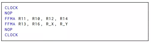
Listing 1: Code used to check Register File read conflicts.
Although NVIDIA has no official tool to write SASS code (NVIDIA assembly language) directly, various third-party tools allow programmers to rearrange and modify assembly instructions (including control bits). These tools are used, for example, to optimize performance in critical kernels when the compiler generated code is not optimal. MaxAS [36] was the first tool for modifying SASS binaries. Later on, other tools such as KeplerAS [93, 94] were developed for Kepler architecture. Then, TuringAS [90] and CUAssembler [29] appeared to support more recent architectures. We have decided to use CUAssembler due to its flexibility, extensibility, and support for the latest hardware.
4. Control Bits in Modern NVIDIA GPU Architectures
The ISA of modern NVIDIA GPU architectures contains control bits and information that the compiler provides to maintain correctness. Unlike GPU architectures in previous works that check data dependence by tracking register reads and writes at run time (see section 2), these GPU architectures rely on the compiler to handle register data dependencies [62]. For this purpose, all as-sembly instructions include some control bits to properly manage dependencies in addition to improving performance and energy consumption.
Below, we describe the behavior of these control bits included in every instruction. The explanation is based on some documents [29, 36, 43, 44], but these documents are often ambiguous or incomplete, so we use the methodology described in section 3 to uncover the semantics of these control bits and verify that they act as described below.
Sub-cores can issue a single instruction per cycle. By default, the Issue Scheduler tries to issue instructions of the same warp if the oldest instruction in the program order of that warp is ready. The compiler indicates when an instruction will be ready for issue using the control bits. If the oldest instruction of the warp that issued an instruction in the previous cycle is not ready, the issue logic selects an instruction from another warp, following the policy described in subsection 5.1.
To handle producer-consumer dependencies of fixed-latency instructions, each warp has a counter that is referred to as Stall counter. If this counter is not zero, this warp is not candidate to issue instructions. The compiler sets this counter with the latency of the producing instruction minus the number of instructions between the producer and the first consumer. All these per-warp Stall counters are decreased by one every cycle until they reach 0. The issue logic will simply check this counter and will not consider issuing another instruction of the same warp until its value is zero. For example, an addition whose latency is four cycles and its first consumer is the following instruction encodes a four in the Stall counter. Using the methodology explained in section 3, we have verified that if the Stall counter is not properly set, the result of the program is incorrect since the hardware does not check for RAW hazards, and simply relies on these compiler-set counters. In addition, this mechanism has benefits in terms of area and energy wiring. Keep in mind that wires from fixed-latency units to the dependence handling components are not needed, in contrast to a traditional scoreboard approach where they are required.
Another control bit is called Yield, and is used to indicate the hardware that in the next cycle it should not issue and instruction of the same warp. If the rest of the warps of the sub-core are not ready in the next cycle, no instruction is issued.
Each instruction sets the Stall counter and the Yield bit. If the Stall counter is greater than one, the warp will stall for at least one cycle, so in this case, no matter whether Yield is set or not.
On the other hand, some instructions (e.g., memory, special functions) have variable latency, and the compiler does not know their execution time. Therefore, the compiler cannot handle these hazards through the Stall counter. These hazards are resolved through Dependence counters bits. Each warp has six special registers to store these counters, which are referred to as SBx with x taking a value in the range [0 − 5]. Each of these counters can count up to 63.
These counters are initialized to zero when a warp starts. To handle a producer-consumer dependence, the producer increases a particular counter after issue, and decreases it at write-back. The consumer instruction is instructed to stall until this counter is zero.
For WAR hazards, the mechanism is similar, with the only difference being that the counter is decreased after the instruction reads its source operands, instead of decreasing the counter at write-back.
In each instruction, there are some control bits to indicate up to two counters that are increased at issue. One of these counters will be decreased at write-back (to handle RAW and WAW dependencies) and the other at register read (to handle WAR dependencies). For this purpose, every instruction has two fields of 3 bits each to indicate these two counters. Besides, every instruction has a mask of 6 bits to indicate which dependence counters it has to check to determine if it is ready for issue. Note that an instruction can check up to all six counters.
Consider that if an instruction has multiple source operands whose producers have variable latency, the same Dependence counter can be used by all these producers without losing any parallelism. It is important to note that this mechanism may encounter limits of parallelism in scenarios where there are more than six consumer instructions with different variable-latency producers. In such cases, the compiler must choose between two alternatives to manage the situation: 1) group more instructions under the same Dependence counter, or 2) reorder the instructions differently
The incrementing of the Dependence counters is performed the cycle after issuing the producer instruction, so it is not effective until one cycle later. Therefore, if the consumer is the next instruction, the producer has to set the Stall counter to 2, to avoid issuing the consumer instruction the following cycle.
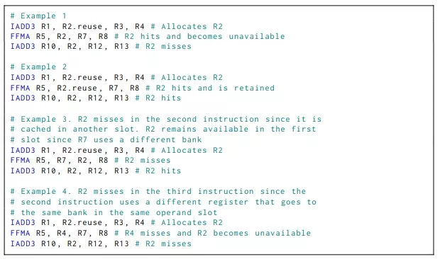
An example of handling dependencies with variable-latency producers can be found in Figure 2. This code shows a sequence of four instructions (three loads and one addition) with its associated encoding. As the addition has dependencies with the loads (variablelatency instructions), Dependence counters are used to prevent data hazards. The instruction at PC 0x80 has RAW dependencies with instructions at 0x50 and 0x60. Thus, SB3 is incremented by instructions 0x50 and 0x60 at issue and decremented at write-back. On the other hand, the addition has WAR dependencies with instructions at 0x60 and 0x70. In consequence, SB0 is increased by instructions 0x60 and 0x70 at issue and decreased after reading their respective register source operands. Finally, the Dependence counters mask of the addition encodes that before being issued, SB0 and SB3 must be 0. Note that instruction 0x70 also uses SB4 to control RAW/WAR hazards with future instructions, but instruction 0x80 does not wait for this Dependence counter since it does not have any dependence with that load. Clearing WAR dependencies after reading the source operands is an important optimization, since source operands are sometimes read much earlier than the result is produced, especially for memory instructions. For instance, in this example, instruction 0x80 waits until instruction 0x70 reads R2 for clearing this WAR dependence, instead of waiting until instruction 0x70 performs its write-back, which may happen hundreds of cycles later.
An alternative way of checking the readiness of these counters is through the DEPBAR.LE instruction. As an example, DEPBAR.LE SB1, 0x3, {4,3,2}, requires the Dependence counter SB1 to have a value less or equal to 3 to continue with the execution. The last argument ([, {4,3,2}]) is optional, and if used, the instruction cannot be issued until the values of the Dependence counters specified by those IDs (4, 3, 2 in this example) are equal to 0.
DEPBAR.LE can be especially useful in some particular scenarios. For instance, it allows the use of the same Dependence counter for a sequence of 𝑁 variable-latency instructions that perform their write-back in order (e.g., memory instructions with the STRONG.SM modifier) when a consumer needs to wait for the first 𝑀 instructions. Using a DEPBAR.LE with its argument equal to 𝑁 − 𝑀 makes this instruction wait for the 𝑀 first instructions of the sequence. Another example is to reuse the same Dependence counter to protect RAW/WAW and WAR hazards. If an instruction uses the same Dependence counter for both types of hazards, as WAR hazards are resolved earlier than RAW/WAW, a following DEPBAR.LE SBx, 0x1 will wait until the WAR is solved and allow the warp to continue its execution. A later instruction that consumes its result needs to wait until this Dependence counter becomes zero, which means that the results have been written.
Additionally, GPUs have a register file cache used to save energy and reduce contention in the register file read ports. This structure is software-managed by adding a control bit to each source operand, the reuse bit, which indicates the hardware whether to cache or not the content of the register. More details about the organization of register file cache are explained in section 5.3.1.
Finally, although this paper focuses on NVIDIA architectures, exploring AMD GPU ISAs documentation [6–15] reveals that AMD also relies on a hardware-software codesign to manage dependencies and boost performance. Similar to NVIDIA’s DEPBAR.LE instruction, AMD employs a waitcnt instruction; depending on the architecture, each wavefront (warp) has three or four counters, with each counter dedicated to specific instruction types and its use required to protect data hazards created by those instructions. AMD does not allow regular instructions to wait for a counter to reach zero using control bits, requiring an explicit waitcnt instruction instead, which increases the number of instructions. This design reduces the decoding overhead, yet increases the overall instruction count. In contrast, NVIDIA’s alternative enables more concurrent dependence chains even within the same instruction type, as it has up to two counters more per warp, and the counters are not tied to any instruction type. Although AMD does not need software or compiler intervention to avoid data hazards with ALU instructions, it introduced the DELAY_ALU instruction in RDNA 3/3.5 architectures [13, 15] to mitigate pipeline stalls caused by dependencies. Conversely, NVIDIA depends on the compiler to correctly handle data dependencies by setting the Stall counter for fixed-latency producers, resulting in a lower instruction count but higher decoding overhead.
5 GPU cores Microarchitecture
In this section, we describe our findings regarding the microarchitecture of GPU cores of modern commercial NVIDIA GPUs, using the methodology explained in section 3. Figure 3 shows the main components of the GPU cores’ microarchitecture. Below, we de-scribe in detail the microarchitecture of the issue scheduler, the front-end, the register file, and the memory pipeline.
5.1 Issue Scheduler
In this subsection we dissect the Issue Scheduler of modern NVIDIA GPUs. First, we describe which warps are considered candidates for issue every cycle in subsubsection 5.1.1. Then, we present the Selection policy in subsubsection 5.1.2.
5.1.1 Warp Readiness.
A warp is considered a candidate for issuing its oldest instruction in a given cycle if some conditions are met. Some of these conditions depend on previous instructions of the same warp, while others rely on the global state of the core.
An obvious condition is having a valid instruction in the Instruction Buffer. Another condition is that the oldest instruction of the warp must not have any data dependence hazard with older instructions of the same warp not yet completed. Dependencies among instructions are handled through software support by means of the control bits described above in section 4.
Besides, for fixed-latency instructions, a warp is candidate to issue its oldest instruction in a given cycle only if it can be guaranteed that all needed resources for its execution will be available once issued.
One of these resources is the execution unit. Execution units have an input latch that must be free when the instruction reaches the execution stage. This latch is occupied for two cycles if the width of the execution unit is just half warp, and for one cycle if its width is a full warp.
For instructions that have a source operand in the Constant Cache, the tag look-up is performed in the issue stage. When the oldest instruction of the selected warp requires an operand from the constant cache and the operand is not in the cache, the scheduler does not issue any instruction until the miss is serviced. However, if the miss has not been served after four cycles, then the scheduler switches to a different warp (the youngest with a ready instruction).
As for the availability of read ports in the register file, the issue scheduler is unaware of whether the evaluated instructions have enough ports for reading without stalls in the following cycles. We have reached this conclusion after observing that the conflicts in the code shown in Listing 1 do not stall the issue of the second CLOCK if we remove the NOP between the last FFMA and the last CLOCK instruction. We performed a multitude of experiments to unveil the pipeline structure between issue and execute, and we could not find a model that perfectly fits all the experiments. However, the model that we describe below is correct for almost all the cases, so it is the model that we assume. In this model, fixed-latency instructions have two intermediate stages between the Issue stage and the stage(s) for reading source operands. The first stage, which we call Control, is common for fixed and variable latency instructions, and its duty is to increase the Dependence counters or read the value of the clock counter if needed. This causes, as corroborated by our experiments, that an instruction that increases the Dependence counter and the instruction that waits until that Dependence counter is 0 requires at least one cycle in between to make visible that increase, so two consecutive instructions cannot use Dependence counters to avoid data dependence hazards unless the first instruction sets the Yield bit or a Stall counter bigger than one.
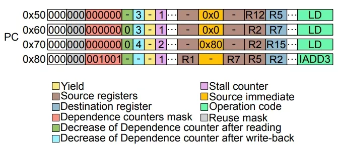
Figure 2: Example of using Dependence counters to handle dependencies.
The second stage only exists for fixed-latency instructions. In this stage, the availability of register file read ports is checked, and the instruction is stalled in this stage until it is guaranteed that it can proceed without any register file port conflict. We call this stage Allocate. More details about the register file read and write pipeline and its cache are provided in subsection 5.3.
Variable-latency instructions (e.g., memory instructions) are de-livered directly to a queue after going through the Control stage (without going through the Allocate stage). Instructions in this queue are allowed to proceed to the register file read pipeline when they are guaranteed not to have any conflict. Fixed-latency instruc-tionsaregivenpriorityovervariable-latencyinstructionstoallocate register file ports, as they need to be completed in a fixed number of cycles after issue to guarantee the correctness of the code, since dependencies are handled by software as described above.
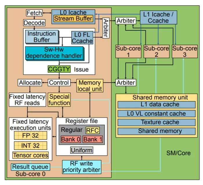
Figure 3: Modern NVIDIA GPU SM/Core design.
5.1.2 Scheduling Policy.
To discover the policy of the issue scheduler, we developed many different test cases involving multiple warps and recorded which warp was chosen for issue in each cycle by the issue scheduler. This information was gathered through instructions that allow to save the current CLOCK cycle of the GPU. However, as the hardware does not allow issuing two of these instructions consecutively, we employed a controlled number of other instructions in between (normally NOPs). We also varied the specific values in the Yield and the Stall counter control bits.
Our experiments allowed us to conclude that the warp scheduler uses a greedy policy that selects an instruction from the same warp if it meets the eligibility criteria described above. When switching to a different warp, the youngest one that meets the eligibility criteria is selected.
This issue scheduler policy is illustrated with some examples of our experiments in Figure 4. This figure depicts the issue of instructions when four warps are executed in the same sub-core for three different cases. Each warp executes the same code composed of 32 independent instructions that can be issued one per cycle.
In the first case, Figure 4 a , all Stall counters, Dependence masks and Yield bits are set to zero. The scheduler starts issuing instructions from the youngest warp, which is W3, until it misses in the Icache. As a result of the miss, W3 does not have any valid instruction, so the scheduler switches to issue instructions from W2. W2 hits in the Icache since it reuses the instructions brought by W3, and when it reaches the point where W3 missed, the miss has already been served, and all remaining instructions are found in the Icache, so the scheduler greedily issues that warp until the end. Later, the scheduler proceeds to issue instruction from W3 (the youngest warp) until the end, since now all instructions are present in the Icache. Then, the scheduler switches to issue instructions from W1 from beginning to end, and finally, it does the same for W0 (the oldest warp).
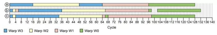
Figure 4: Timelines of the issue of instructions from four different warps.
Figure 4 b shows the timeline of when instructions are issued when the second instruction of each warp sets its Stall counter to four.WecanobservethattheschedulerswapsfromW3toW2after two cycles, to W1 after another two cycles, and then back to W3 after another two cycles (since W3 Stall counter has become zero). Once W3, W2, and W1 have finished, the scheduler starts issuing from W0. After issuing the second instruction of W0, the scheduler generates four bubbles because it has no other warp to hide the latency imposed by the Stall counter.
Figure 4 c shows the scheduler’s behavior when Yield is set in the second instruction of each warp. We can see that the scheduler switches to the youngest among the rest of the warps after issuing the second instruction of each warp. For instance, W3 switches to W2, and W2 switches back to W3. We also tested a scenario where Yield is set and no more warps are available (not shown in this figure), and we observed that the scheduler generates a bubble of one cycle.
We call this issue scheduler policy Compiler Guided Greedy Then Youngest (CGGTY) since the compiler assists the scheduler by means of the control bits: Stall counter, Yield and Depencence counters.
However, we have only confirmed this behavior for warps within the same CTA, as we have not yet devised a reliable methodology to analyze interactions among warps from different CTAs.
5.2 Front-end
According to diagrams in multiple NVIDIA documents [20, 28, 65– 69], SMs have four different sub-cores and warps are evenly dis-tributed among sub-cores in a round robin manner (i.e., warp ID %4) [43, 44]. Each sub-core has a private L0 instruction cache that is connected to an L1 instruction cache that is shared among all four sub-cores of the SM. We assume there is an arbiter for dealing with the multiple requests of different sub-cores.
Each L0 Icache has an instruction prefetcher [60]. Our experiments corroborate previous studies by Cao et al. [24] that demonstrated that instruction prefetching is effective in GPUs. Although we have not been able to confirm the concrete design used in NVIDIA GPUs, we suspect it is a simple scheme like a stream buffer [47] that prefetches successive memory blocks when a miss occurs. We assume that the stream buffer size is 16 based on our analysis, as detailed in subsection 7.3.
We could not confirm the exact instruction fetch policy with our experiments, but it has to be similar to the issue policy; otherwise, the condition of not finding a valid instruction in the Instruction Buffer would happen relatively often, and we have not observed this in our experiments. Based on that, we assume that each sub-core can fetch and decode one instruction per cycle. The fetch scheduler tries to fetch an instruction from the same warp that has been issued in the previous cycle (or the latest cycle in which an instruction was issued) unless it detects that the number of instructions already in the Instruction Buffer plus its in-flight fetches are equal to the Instruction Buffer size. In this case, it switches to the youngest warp with free entries in its Instruction Buffer. We assume an Instruction Buffer with three entries per warp since this is enough to support the greedy nature given that there are two pipeline stages from fetch to issue. Were the Instruction Buffer of size two, the Greedy policy of the issue scheduler would fail. For example, assume a scenario in which the Instruction Buffer has a size of two and all the requests hit in the Icache, all warps have their Instruction Buffer full, and in cycle 1, a sub-core is issuing instructions from warp W1 and fetching from W0. In cycle 2, the second instruction of W1 will be issued, and the third instruction will be fetched. In cycle 3, W1 will have no instructions in its Instruction Buffer because instruction 3 is still in the decode. Therefore, its greedy behavior would fail, and it would have to switch to issue from another warp. Note that this would not happen in case of having three entries in the Instruction Buffer, as corroborated by our experiments. Note that most previous designs in the literature normally assume a fetch and decode width of two instructions and an Instruction Buffer of two entries per warp. In addition, those designs only fetch instructions when the Instruction Buffer is empty. Thus, the greedy warp always changes at least after two consecutive instructions, which does not match our experimental observations.
5.3. Register File
We have performed a multitude of experiments by running different combinations of SASS assembly instructions to unveil the register file organization. For example, we wrote codes with different pressure on the register file ports, with and without using the register file cache.
Modern NVIDIA GPUs have various register files:
- Regular: Recent NVIDIA architectures have 65536 32-bit registers per SM [65–69] used to store the values operated by threads. The registers are arranged in groups of 32, each group corresponding to the registers of the 32 threads in a warp, resulting in 2048 warp registers. These registers are evenly distributed between sub-cores, and the registers in each sub-core are organized in two banks [43, 44]. The number of registers used by a particular warp can vary from 1 to 256, and it is decided at compile time. The more registers used per warp, the fewer warps can run parallel in the SM.
- Uniform: Each warp has 64 private, 32-bit registers that store values shared by all the threads of the warp [43].
- Predicate: Each warp has eight 32-bit registers, each bit being used by a different thread of the warp. These predicates are used by warp instructions to indicate which threads must execute the instruction and, in the case of branches, which threads must take the branch and which ones not.Uniform Predicate: Each warp has eight 1-bit registers that store a predicate shared by all the treads in the warp.
- SB Registers: As described in section 4, each warp has six registers, called Dependence counters, that are used to track variable-latency dependencies.
- B Registers: Each warp has at least 16 B registers for man-aging control flow re-convergence [79].
- Special Registers: Various other registers are used to store special values, such as the thread or block IDs.
Unlike previous works [1, 18, 49] that assume the presence of an operand collector to deal with conflicts in the register file ports, modern NVIDIA GPUs do not make use of it. Operand collector units would introduce variability in the elapsed time between issue and write-back, making it impossible to have fixed-latency instructions for the NVIDIA ISA, whose latency must be known at compile time to handle dependencies correctly as explained section 4. We have confirmed the absence of operand collectors by checking the correctness of specific producer-consumer sequences of instructions when varying the number of operands that go to the same bank. We observed that regardless of the number of register file port conflicts, the value required in the Stall counter field of instructions to avoid data hazards and the elapsed time to execute the instruction remains constant.
Our experiments revealed that each register file bank has a dedicated write port of 1024 bits. Besides, when a load instruction and a fixed-latency instruction finish at the same cycle, the one that is delayed one cycle is the load instruction. On the other hand, when there is a conflict between two fixed latency instructions, for instance, a IADD3 followed by an IMAD that uses the same destination bank, none of them is delayed. This implies the use of a result queue like the one introduced in Fermi [61] for fixed-latency instructions. The consumers of these instructions are not delayed, which implies the use of bypassing to forward the results to the consumer before being written in the register file.
Regarding reads, we have observed a bandwidth of 1024 bits per bank. The measurements were obtained through various tests that recorded the elapsed time of consecutive FADD, FMUL, and FFMA instructions 1 . For instance, FMUL instructions with both source operands in the same bank create a 1-cycle bubble, whereas if the two operands are in different banks, there is no bubble. FFMA instructions with all three source operands in the same bank generate a 2-cycle bubble.
Unfortunately, we could not find a read policy that matches all the cases we have studied, as we observed that the generation of bubbles depends on the type of instructions and the task of each operand in the instructions. We found that the best approximation that matches almost all the experiments we tested is a scheme with two intermediate stages between the instruction issue and operand read of fixed-latency instructions, which we call Control and Allocate. The former has been explained in subsubsection 5.1.1. The latter is in charge of reserving the register file read ports. Each bank of the register file has one read port of 1024 bits, and read conflicts are alleviated by using a register file cache (more details later). Our experiments showed that all the fixed-latency instructions spend three cycles for reading source operands, even if some of these cycles the instruction is idle (for instance when there are only two source operands) because FADD and FMUL have the same latency as the FFMA despite having one operand less, and FFMA always has the same latency regardless of whether its three operands are in the same bank or not. If the instruction in the allocate stage realizes that it cannot read all its operands in the next three cycles, it is held in this stage (stalling the pipeline upwards) and generates bubbles until it can reserve all ports needed to read the source operands in the next three cycles.
5.3.1. Register file cache.
The use of a Register file cache (RFC) in GPUs has been investigated for relieving contention in the Register File ports and saving energy [2, 30, 32, 33, 78].
Through our experiments, we observed that the NVIDIA design is similar to the work of Gebhart et al. [33]. In line with that design, the RFC is controlled by the compiler and is only used by instruc-tionsthathaveoperandsintheRegularRegisterFile.Regardingthe Last Result File structure, what we call the result queue behaves similarly. However, unlike the above-cited paper, a two-level issue scheduler is not used, as explained above in subsubsection 5.1.2.
Regarding the organization of the RFC, our experiments showed that it has one entry for each of the two register file banks in each sub-core. Each entry stores three 1024-bit values, each corresponding to one of the three regular register source operands that instructions may have. Overall, the RFC’s total capacity is six 1024- bit operand values (sub-entries). Note that there are instructions that have some operands that require two consecutive registers (e.g., tensor core instructions). In this case, each of these two registers come from a different bank, and are cached in their corresponding entries.
The compiler manages the allocation policy. When an instruction is issued and reads its operands, each operand is stored in the RFC if the compiler has set its reuse bit for that operand. A subsequent instruction will obtain its register source operand from the RFC if the instruction is from the same warp, the register ID coincides with the one stored in the RFC, and the operand position in the instruction is the same as in the instruction that has triggered the caching. A cached value is unavailable after a read request arrives to the same bank and operand position, regardless of whether it hits in the RFC. This is illustrated in example 2 of Listing 2; to allow the third instruction to find R2 in the cache, the second instruction must set the reuse bit of R2 in spite of R2 being already in the cache for the second instruction. Listing 2 shows three other examples to illustrate the RFC behavior.
Listing 2: Register file cache behavior.
5.4. Memory Pipeline
The memory pipeline in modern NVIDIA GPUs has some initial stages local to each sub-core, whereas the last stages that perform the memory access are shared by the four sub-cores since the data cache and the shared memory are shared by them [20, 28]. In this section, we discover the size of the load/store queues in each sub-core, the rate at which each sub-core can send requests to the shared memory structures, and the latency of the different memory instructions.
Note that there are two main types of memory accesses, those that go to shared memory (the SM local memory shared among all threads in a block) and those that go to the global memory (the GPU main memory).
To discover the size of the queues and the memory bandwidth, we run a set of experiments in which each sub-core either executes a warp or is idle. Each warp executes a sequence of independent loads or stores that always hit in the data cache or shared memory and use regular registers. Table 1 shows the results of these experiments. The first column shows the instruction number in the code, and the next four columns show in which cycle this instruction is issued in each of the cores for four different scenarios that differ in the number of active cores.
We can observe that each sub-core can issue one instruction per cycle for five consecutive memory instructions in Ampere. The issueofthe6thmemoryinstructionisstalledforanumberofcycles that depend on the number of active sub-cores. From these data, we can infer that each sub-core can buffer up to five consecutive instructions without stalling, and the global structures can receive a memory request every two cycles from any of the sub-cores. For instance, if we look at the cases with multiple active sub-cores, we can see that the 6th and following instructions of each sub-core are issued every other two cycles.
We can also infer that the address calculation done in each sub-core has a throughput of one instruction every four cycles, as demonstrated by the 4-cycle gap in the issue after the 6th instruction when there is a single active sub-core. When two sub-cores are active, each can issue a memory instruction every 4 cycles since the shared-structures can handle one instruction every two cycles. When more sub-cores are active, the shared-structures become the bottleneck. For instance, when four sub-cores are active, each sub-core can issue an instruction only every 8 cycles since the shared-structures only allow one instruction every two cycles as its maximum throughput.
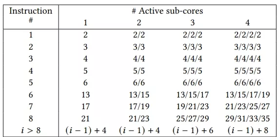
Table 1: Cycle in which each memory instruction is issued. Each cell stores the cycle for all active sub-cores sorted by cycles in ascending order.
Regarding the size of the memory queue in each sub-core, we estimate that it has a size of four even though each sub-core can buffer five consecutive instructions. The instruction reserves the slot when it arrives at the unit and frees it when it leaves the unit.
As regards latencies, we measured two different latencies for each instruction type when the instruction hits in the cache and there is a single thread in execution. The first latency is the elapsed time since a load is issued until the earliest time that a consumer or an instruction that overwrites the same destination register can issue. We refer to this as RAW/WAW latency (note that stores cannot generate register RAW/WAW dependencies). The second one is the elapsed time since a load or store is issued until the earliest time that an instruction that writes in a source register of the load/store can be issued. We refer to this time as WAR latency. The results are shown in Table 2.
We can see that global memory accesses are faster if instructions use uniform registers for computing their addresses rather than regular registers. This difference is due to a faster address calculation. When using uniform registers, all threads in a warp share the same register, and thus, a single memory address needs to be computed. On the other hand, when using regular registers, each thread needs to compute a potentially different memory address.
We can also observe that the latency of shared memory loads is lower than that of global memory. We can also observe that their WAR latency is the same for regular and uniform registers, whereas their RAW/WAW latency is one cycle lower for uniform registers. The fact that WAR latencies are equal for regular and uniform registers suggests that the address calculation for shared memory is done in the shared-structures, rather than in the local sub-core structures, so the WAR dependence is released once the source registers are read.
As expected, latencies also depend on the size of the read/written values. For WAR dependencies, the latency of loads does not change since the source operands are only for address calculation and thus, they are always the same size no matter the size of the loaded value. For store instructions, WAR latencies increase with the size of the written value to memory since this value is a source operand that also needs to be read from the register file. For RAW/WAW dependencies (only apply to loads), latencies increase as we increase the size of the read value, since more data needs to be transferred from the memory to the register file. We have measured that the bandwidth for this transfer is 512 bits per cycle.
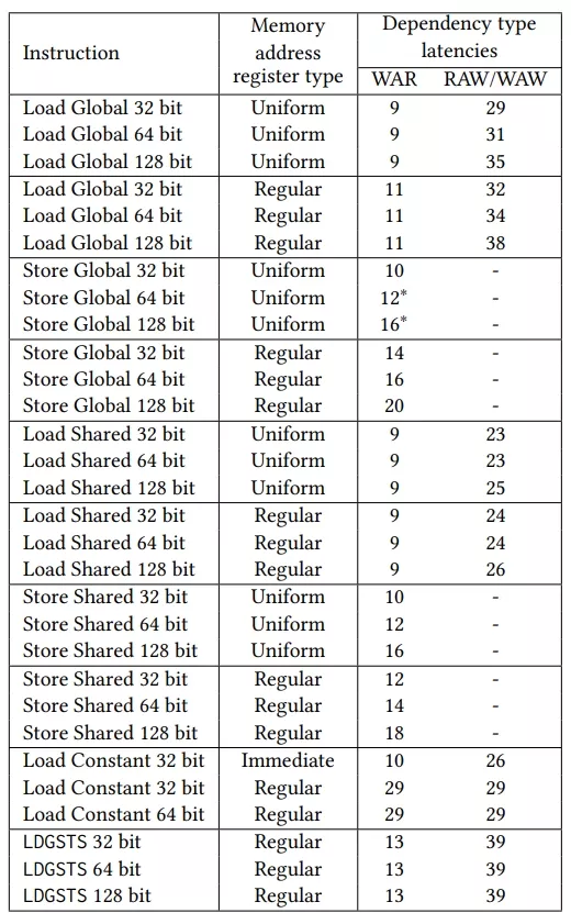
Table 2: Memory instructions latencies in cycles. Values with ∗ are approximations as we were unable to gather these data.
In addition, we can observe that the constant cache’s WAR latency is significantly greater than loads to the global memory, whereas RAW/WAW latencies are a bit lower. We could not con-firm any hypothesis that explains this observation. However, we discovered that accesses to the constant memory done by fixed-latency instructions go to a different cache level than load constant instructions. We confirmed this by preloading a given address into the constant cache through an LDC instruction and waiting for the instruction until it is complete. Then, we issued a fixed-latency instruction using the same constant memory address and measured that the issue was delayed 79 cycles, which corresponds to a miss, instead of causing no delay, which would correspond to a hit. Therefore, fixed-latency instructions accessing the constant address space use the L0 FL (fixed latency) constant cache, while accesses made through LDC instructions utilize the L0 VL (variable latency) constant cache.
Finally, we analyze LDGSTS instruction, which was introduced to reduce the pressure of the register file and improve the efficiency of transferring data to the GPU [38]. It loads data from global memory and stores it directly into the shared memory without going through the register file, which saves instructions and registers. We can see that its latency is the same regardless of the granularity of the instruction. WAR dependencies have the same latency for all granularities since they are released when the address is computed. The RAW/WAR dependency is released when the instruction’s read step has finished, regardless of the instruction’s granularity.
6. Modeling
We have designed from scratch the SM/core model of the Accel-sim framework simulator [49] by modifying the pipeline to implement all the details explained in section 4, section 5 and depicted in Figure 3. The main new components are outlined below.
First, we have added an L0 instruction cache with a stream buffer prefetcher for each sub-core. L0 instruction and constant caches are connected with a parameterized latency to an L1 instruction/- constant cache. We have chosen the size of caches, hierarchy, and latencies according to previous measurements done or the Ampere architecture described by Jia et al [45].
We have modified the Issue stage to support the control bits, the tag look-up to the newly added L0 constant caches for fixed-latency instructions, and the new CGGTY issue scheduler. We included the control stage, in which instructions increase the dependence counters, and the Allocate stage, in which fixed-latency instructions check for conflicts in the access to the register file and the register file cache.
Regarding memory instructions, we have modeled a new unit per sub-core and a unit shared among sub-cores, with the latencies presented in the previous section.
Additionally, as Abdelkhalik et al. [3] have demonstrated that the latency of a tensor core instruction depends on its operand’s numeric types and sizes, so we have adapted the model to use the correct latency for each operand type and size.
Other details that we have modeled are the execution pipeline shared by all sub-cores for double precision instructions in architectures without dedicated double precision execution units in each sub-core. Moreover, we accurately model the timing for reading/writing operands that use multiple registers, which was previously approximated by using just one register per operand. Furthermore, we fixed some inaccuracies in instruction addresses reported in a previous work [40].
Apart from implementing the new SM/core model in the simulator, we have extended the tracer tool. The tool has been extended to dump the ID of all types of operands (regular registers, uniform registers, predication registers, immediate, etc.). Another important extension is the capability to obtain the control bits of all instructions since NVBit does not provide access to them. This is done by obtaining the SASS through the CUDA binary utilities [70] at compile time. This implies modifying the compilation of the applications to generate microarchitecture-dependent code at compile time instead of using a just-in-time compilation approach. Unfortunately, for a few kernels (all of them belonging to Deepbench), NVIDIA tools do not provide the SASS code, which prevents obtaining the control bits for these instructions. To simulate these applications, we use a hybrid mode for dependencies where traditional scoreboards are employed in kernels that do not have the SASS code; otherwise, control bits are used.
We have extended the tool to capture memory accesses to the constant cache or global memory through descriptors. Despite the latter type of accesses being claimed to be introduced in Hopper [70], we have noticed that Ampere already uses them. Descriptors are a new way of encoding memory references that uses two operands. The first operand is a uniform register to encode the semantics of the memory instruction, while the second encodes the address. We have extended the tracer to capture the address. Unfortunately, the behavior encoded in the uniform register remains untracked.
We plan to make public all the simulator and tracer changes made in the Accel-sim framework.
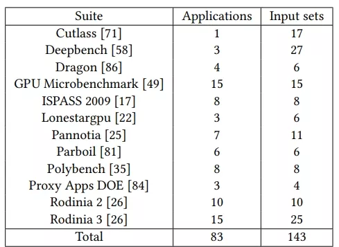
Table 3: Benchmarks suites.
7. Validation
In this section, we evaluate the accuracy of our proposed microarchitecture for the GPU cores. First, we describe the methodology that we have followed in subsection 7.1. Then, we validate the design in subsection 7.2. Next, we examine the impact of the register file cache and the number of register file read ports on accuracy and performance in subsection 7.4. Later, we study the impact of two different components in the design, such as the instruction prefetcher in subsection 7.3 and an analysis of the dependence checking mechanisms in subsection 7.5. Finally, we discuss how the model can be seamlessly adapted for NVIDIA architectures other than Ampere in subsection 7.6
7.1. Methodology
We validate the accuracy of the proposed GPU core by comparing the results of our version of the simulator against hardware countermetrics obtained in a real GPU. We use four different Ampere [67] GPUs whose specifications are shown in Table 4. All the GPUs use CUDA 11.4 and NVBit 1.5.5. We also compare our model/simulator with the vanilla Accel-sim simulator framework, since our model is built on top of it.
We use a wide variety of benchmarks from 12 different suites. A list of the suites that have been employed and the number of appli-cationsanddifferentinputdatasetscanbefoundinTable3.Intotal, we use 143 benchmarks, 83 of those being different applications, and the rest corresponding to just changing the input parameters.
7.2. Performance Accuracy
Table 4 shows the reported mean percentage absolute error (MAPE) for both models (our model and Accel-sim) with respect to the real hardware for each of the GPUs. We can see that our model is significantly more accurate than Accel-sim in all the evaluated GPUs, and for the biggest GPU, the NVIDIA RTX A6000, the MAPE is less than half that of Accel-sim. Regarding the correlation, both models are very similar, but our model is slightly better.
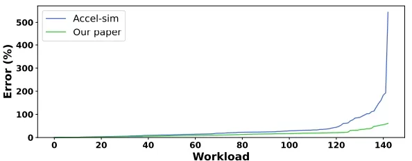
Figure 5: NVIDIA RTX A6000 percentage absolute error for each benchmark. Benchmarks are sorted by error in ascend-ing order in each of the configurations.
Figure 5 shows the APE of both models for the NVIDIA RTX A6000 and each of the 143 benchmarks sorted in increasing error for each of the models. We can see that our model consistently has less absolute percentage error than Accel-sim for all applications, and the difference is quite significant for half of the applications. Moreover, we can observe that Accel-sim has an absolute percent-ageerrorgreaterorequalto100%for10applications,anditreaches 543% in the worst case, whereas our model never has an absolute percentage error greater than 62%. If we look at the 90th percentile as an indication of the tail accuracy, Accel-sim absolute percentage error is 82.64%, whereas it is 31.47% for our model. This proves that our model is significantly more accurate and robust than the Accel-sim model.
7.3. Sensitivity Analysis of Instruction Prefetching
The characteristics of the stream buffer instruction prefetcher have high impact on the global model accuracy. In this section, we analyze the error of different configurations, including disabling the prefetcher, having a perfect instruction cache, and a stream buffer prefetcher with sizes 1, 2, 4, 8, 16, and 32 entries. All the configurations are based on the NVIDIA RTX A6000. The MAPE for each configuration is shown in Table 5. We can see that the best accuracy is obtained with a stream buffer of size 16.
We can draw an additional conclusion from the speed-up results shown in Table 5: a straightforward prefetcher, such as a stream buffer, behaves close to a perfect instruction cache in GPUs. This is because the different warps in each sub-core usually execute the same code region and the code of typical GPGPUs applications do not have a complex control flow, so prefetching 𝑁 subsequent lines usually performs well. Note that since GPUs do not predict branches, it is not worth implementing a Fetch Directed Instruction prefetcher [76] because it would require the addition of a branch predictor.
Regarding simulation accuracy, we conclude that when instruction cache enhancements are not under investigation, using a perfect instruction cache usually yields comparable accuracy with faster simulation speeds. However, for benchmarks where control flow is relevant —such as dwt2d [26], lud [26], or nw [26]— employing a perfect instruction cache or omitting stream buffers results in significant inaccuracies (more than 20% difference compared to a perfect instruction cache and more than 200% respect to an instruction cache without prefetching). This inaccuracy arises because a perfect instruction cache fails to capture the performance penalties incurred by frequent jumps between different code segments, while the absence of prefetching overly penalizes the execution of other parts of the program, which also reveals that there is an opportunity for improvement in those benchmarks.
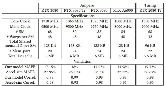
Table 4: GPUs specifications and performance accuracy.
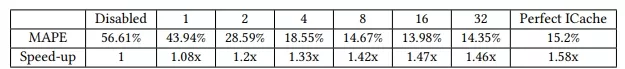
Table 5: MAPE of different prefetcher configurations in the NVIDIA RTX A6000 and speed-up of each configuration with respect to prefetching disabled.
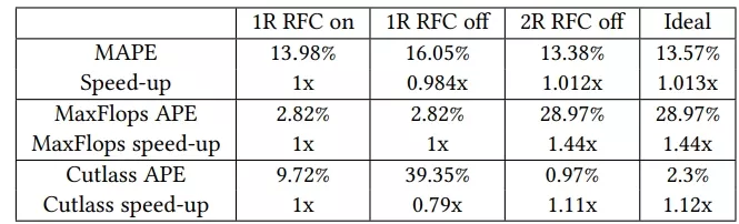
Table 6: MAPE of different RF configurations in the NVIDIA RTX A6000 and speed-up of each configuration with respect to the baseline (1 read port and RFC enabled).
7.4. Sensitivity Analysis of the Register File Architecture
Table 6 illustrates how the presence of a register file cache and an increased number of register file read ports per bank affect simulation accuracy and performance. It also shows the results for an Ideal scenario where all operands can be retrieved in a single cycle. The average performance and accuracy across all benchmarks are similar for all configurations. However, a closer examination of specific benchmarks —such as the compute-bound MaxFlops (Accel-sim GPU Microbenchmark) [49] and Cutlass [71] configured with the sgemm parameter —reveals more nuanced behavior. Both benchmarks rely heavily on fixed-latency arithmetic instructions, which are particularly sensitive to stalls caused by register file access limitations because they typically use three operands per instruction.
For MaxFlops, performance is identical regardless of whether the RFC is present, since only one static instruction makes use of it. Notably, performance improves dramatically by approximately 44% when two read ports per register file bank are employed. This improvement is logical given that three operands per instruction are common and four read ports (two per bank) are sufficient to meet demand. In contrast, from a simulation accuracy perspective, the configuration of the two read ports exhibits a significant deviation.
In the case of Cutlass with sgemm, a single-port configuration without a register file cache leads to a substantial performance degradation (0.78x). This performance drop is consistent with the observation that 35.9% of the static instructions in the program make use of the register file cache in at least one of their operands. However, introducing a register file with two read ports per bank yields a 12% performance improvement, which suggests that there is room for improvement in the organization of the register file and its cache.
In summary, the register file architecture, including its cache, has an important effect on individual benchmarks, so its accurate model is important. A single port per bank plus a simple cache performs close to a register file with an unbounded number of ports on average, but for some individual benchmarks the gap is significant, which suggests that this may be an interesting area for research.
7.5. Analyzing Dependence Management Mechanisms
In this subsection, we analyze the impact on performance and the area of the software-hardware dependence handling mechanism explained in this paper and compare them with the traditional scoreboard method used by former GPUs. Table 7 shows the results for both metrics. Area overhead is reported relative to the area of the regular register file of an SM, which is 256 KB.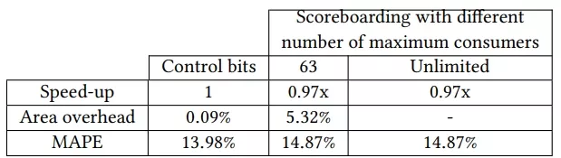
Table 7: Speed-up, area overhead and MAPE of different dependence management mechanisms.
A mechanism based on the traditional scoreboard requires as many entries as registers that can be written, that is, 332 entries per warp (255 for the regular registers, 63 for the uniform registers, 7 for the predicate registers, and 7 for the uniform predicate registers). Additionally, two scoreboards are needed: one for WAW/RAW hazards and another for WAR hazards [57], because even though issue is in-order, the read-write of operands may occur out-of-order due to variable-latency instructions. WAR hazards may occur because variable-latency instructions, such as memory instructions, are queued after being issued and may read their source operands after a younger arithmetic instruction writes its result. While the first scoreboard requires only a single bit per entry, the second one requires more hardware as the number of consumers per entry increases. Assuming support for up to 63 consumers per entry, a single warp would require 2324 bits (332 + 332 × 𝑙𝑜𝑔2(63 + 1)) for dependency handling. For the entire SM, this translates to 111,552 bits, which is 5.32% of the register file size.
In contrast, the software-hardware mechanism presented in this paper requires six Dependence Counters of six bits each, a Stall Counter of four bits, and a yield bit. This amounts to just 41 bits per warp or 1968 bits per SM. In terms of overhead, this is only 0.09% of the register file size, which is much less than the scoreboard alternative.
In summary, the software-hardware codesign based on control bits outperforms other alternatives and it has a negligible area overhead. The difference in overhead with respect to scoreboarding becomes even more significant in GPUs that support up to 64 warps per SM, such as NVIDIA Hopper [69], which has an overhead of 0.13% for the control bits alternative and 7.09% for the scoreboard mechanism with 63 consumers. An additional insight is that using a scoreboard mechanism composed of two scoreboards (one for RAW/WAW and another one for WAR hazards with up to 63 consumers) is comparable in simulation accuracy to using control bits. Therefore, it is a valid alternative for applications that do not expose the values of control bits, such as some kernels of the Deepbench benchmark suite.
7.6. Portability to other NVIDIA architectures
In this paper, we focus on the NVIDIA Ampere architecture. However, the findings we have exposed in the paper apply to other architectures, such as Turing. In addition to reporting results for four Ampere GPUs, Table 4 presents results for a Turing GPU, showing a 6.94% MAPE improvement over Accel-sim for the NVIDIA RTX 2080 Ti .
Although we have validated the model on Turing and Ampere, we believe that our findings remain applicable to other NVIDIA architectures. NVIDIA’s public announcements and SM diagrams indicate that significant architectural changes have been limited to enhancements in Tensor cores, ray-tracing units, and minor features such as distributed shared memory between SMs of the same TPC [69]. Nonetheless, estimating the latencies for some instructions, such as memory, will be necessary to adapt the model to these other architectures.
8. Related Work
Simulators are the primary tool for evaluating ideas in computer architecture in academia and industry [5] due to the low cost of assessing new designs. Moreover, they are a great tool to check if designs are close to actual hardware. GPGPUs are no exception, and a leading vendor such as NVIDIA has exposed part of the process of creating their in-house simulator, NVIDIA Architectural Simulator (NVArchSim or NVAS) [85]. In the academic sphere, there are two popular public-domain simulators. The first one is MGPUSim [83], which models the AMD GCN 3 architecture and targets multi-GPU systems supporting virtual memory. An alternative simulator is the Accel-Sim framework [49], a cycle-accurate state-of-the-art trace-driven simulator supporting CUDA applications that models NVIDIA-like modern architectures, which it is based on the former GPGPU-Sim 3 simulator [17].
In the literature, there are different works that try to reverse en-gineering CPU architectural components, such as the Intel Branch Predictor [92] or Intel cache designs [41, 55] to name just a few.
Regarding NVIDIA GPUs, several works have been pursued to unveil specific components of GPUs. Ahn et al. [4] and Jin et al. [46] target to reverse engineer the Network on Chip of the NVIDIA Volta and Ampere architectures, respectively. Lashgar et al. [50] study NVIDIA Fermi’s and Kepler’s capabilities for handling memory requests. Jia et al. [43, 44] present some cache features such as line size and associativity, the latency of instructions, and some details of the register file of Volta and Turing. Khairy et al. [48] explore the L1 data cache and L2 cache designs of Volta. Abdelkhalik et al. [3] establish the relation between PTX and SASS instructions of Ampere and its execution latency. Regarding tensor cores, different works [31, 43, 44, 53, 54, 72, 82, 91] have investigated their programmability and micro-architecture. TLBs of Turing and Ampere have been reverse-engineered by Zhang et al. [95] with the purpose of realizing an attack on Multi-Instance GPUs. Concerning the control flow of modern NVIDIA GPU architectures, Shoushtary et al. [79] define a plausible semantic for control flow instructions of Turing with just a 1.03% error with respect to real hardware traces. The GPU task scheduler and the interaction with an ARM CPU in the NVIDIA Jetson TX2 are studied by Amert et al. [16]. Finally, Wong et al. [88] describe many components of the early Tesla architecture, such as caches, TLB, SIMT control flow behavior, and Cooperative Thread Array (CTA) barriers
Regarding previous works that focused on other GPU vendors, Gutierrez et al. [37] show that directly employing the AMD GPU machine ISA rather than intermediate languages is crucial for accurately assessing bottlenecks and potential solutions during simulation. Moreover, the GAP tool [42] identifies discrepancies between real AMD GPUs and their gem5 [19] simulated counterparts, which has led to improvements in gem5’s AMD GPU accuracy [73, 74]. Finally, Gera et al. [34] introduce a simulation framework and characterize Intel’s integrated GPUs.
Compiler hints (a.k.a. control bits) have been used in GPUs at least since the NVIDIA Kepler architecture [93, 94]. A description of these control bits was published by Gray et al. [36]. In Kepler, Maxwell, and Pascal architectures, one out of each 3 to 7 instructions is usually a compiler-inserted hint instruction. Jia et al. [43, 44] revealed that newer architectures such as Volta or Turing have increased the instruction bit size from 64 to 128 bits. As a result, newer architectures have shifted from having specific instructions for hints to including the hint bits in each instruction. These bits are intended not only to improve the hardware performance but also to ensure the program’s correctness by preventing data hazards. CPUs have used compiler hints to help hardware make better decisions about how to use the different resources [80]. These hints have been used to support different components of the CPUs, such as data bypass, branch prediction, and caches, among others.
To the best of our knowledge, our work is the first one to unveil the GPU core microarchitecture of modern NVIDIA GPUs and develop an accurate microarchitecture simulation model. Some novel features discovered in our work are: a complete definition of the semantics of the control bits and the microarchitectural changes to support them, the behavior of the issue scheduler, the microarchitecture of the register file and its associated cache, and various aspects of the memory pipeline. These aspects are critical for an accurate modeling of modern NVIDIA GPUs.
9. Conclusion
This paper unveils the industry’s modern NVIDIA GPU microarchitecture by reverse engineering it on real hardware. We dissect the issue stage logic, including analyzing warp readiness conditions and discovering that the issue scheduler among warps follows a CGGTY policy. In addition, we unveil different details of the register file, such as the number of ports and their width. Also, we reveal how the register file cache works. Moreover, this paper exhibits some important characteristics of the memory pipeline, like the size of load/store queues, contention between sub-cores, and how latencies are affected by memory instruction granularity accesses. Furthermore, we analyze the fetch stage and propose one that meets the requirements of modern NVIDIA GPUs.
Additionally, the paper compendiums previous public information about control bits by organizing, explaining it in detail, and extending it.
In addition, we model all these details in a simulator and compare this new model against real hardware, demonstrating that it is closer to reality than the previous models by improving its accuracy in cycles by more than 18.24%.
Besides, we demonstrate that instruction prefetching with a simple stream buffer in GPUs performs well in terms of simulation accuracy and performance, approaching a perfect instruction cache. Also, we show how the dependence management mechanism based on control bits used in modern NVIDIA GPUs outperforms other alternatives, such as traditional scoreboarding.
Finally, we investigate how the register file cache and the number register file read ports affect simulation accuracy and performance.
Overall, we can conclude that GPUs are hardware-compiler codesign where the compiler guides the hardware in handling dependencies and introduces hints that can improve performance and energy
References
[1] Tor M. Aamodt, Wilson Wai Lun Fung, and Timothy G. Rogers. 2018. General-purpose Graphics Processor Architectures. Morgan & Claypool Publishers.
[2] Mojtaba Abaie Shoushtary, Jose Maria Arnau, Jordi Tubella Murgadas, and Antonio Gonzalez. 2024. Memento: An Adaptive, Compiler-Assisted Register File Cache for GPUs. In 2024 ACM/IEEE 51th Annual International Symposium on Computer Architecture (ISCA).
[3] Hamdy Abdelkhalik, Yehia Arafa, Nandakishore Santhi, and Abdel-Hameed A. Badawy. 2022. Demystifying the Nvidia Ampere Architecture through Mi-crobenchmarking and Instruction-level Analysis. In 2022 IEEE High Performance Extreme Computing Conference (HPEC). 1–8. https://doi.org/10.1109/HPEC55821. 2022.9926299
[4] Jaeguk Ahn, Jiho Kim, Hans Kasan, Leila Delshadtehrani, Wonjun Song, Ajay Joshi, and John Kim. 2021. Network-on-Chip Microarchitecture-based Covert Channel in GPUs. In MICRO-54: 54th Annual IEEE/ACM International Sympo-sium on Microarchitecture (Virtual Event, Greece) (MICRO ’21). Association for Computing Machinery, New York, NY, USA, 565–577. https://doi.org/10.1145/ 3466752.3480093
[5] Ayaz Akram and Lina Sawalha. 2019. A Survey of Computer Architecture Simulation Techniques and Tools. IEEE Access 7 (2019), 78120–78145. https: //doi.org/10.1109/ACCESS.2019.2917698
[6] AMD. 2016. AMD Graphics Core Next Architecture, Generation 3. Reference Guide. Technical Report. AMD.
[7] AMD. 2020. "AMD Instinct MI100" Instruction Set Architecture. Reference Guide. Technical Report. AMD.
[8] AMD. 2020. "RDNA 1.0" Instruction Set Architecture. Reference Guide. Technical Report. AMD.
[9] AMD. 2020. "RDNA 2" Instruction Set Architecture. Reference Guide. Technical Report. AMD.
[10] AMD. 2020. Vega 7nm Instruction Set Architecture. Reference Guide. Technical Report. AMD.
[11] AMD. 2020. Vega Instruction Set Architecture. Reference Guide. Technical Report. AMD.
[12] AMD. 2022. "AMD Instinct MI200" Instruction Set Architecture. Reference Guide. Technical Report. AMD.
[13] AMD. 2023. "RDNA 3" Instruction Set Architecture. Reference Guide. Technical Report. AMD.
[14] AMD. 2024. "AMD Instinct MI300" Instruction Set Architecture. Reference Guide. Technical Report. AMD.
[15] AMD. 2024. "RDNA 3.5" Instruction Set Architecture. Reference Guide. Technical Report. AMD.
[16] TanyaAmert,NathanOtterness,MingYang,JamesH.Anderson,andF.Donelson Smith. 2017. GPU Scheduling on the NVIDIA TX2: Hidden Details Revealed. In 2017 IEEE Real-Time Systems Symposium (RTSS). 104–115. https://doi.org/10. 1109/RTSS.2017.00017
[17] Ali Bakhoda, George L. Yuan, Wilson W. L. Fung, Henry Wong, and Tor M. Aamodt. 2009. Analyzing CUDA workloads using a detailed GPU simulator. In 2009 IEEE International Symposium on Performance Analysis of Systems and Software (ISPASS). 163–174. https://doi.org/10.1109/ISPASS.2009.4919648
[18] Aaron Barnes, Fangjia Shen, and Timothy G. Rogers. 2023. Mitigating GPU Core Partitioning Performance Effects. In 2023 IEEE International Symposium on High-Performance Computer Architecture (HPCA). 530–542. https://doi.org/10. 1109/HPCA56546.2023.10070957
[19] Nathan Binkert, Bradford Beckmann, Gabriel Black, Steven K. Reinhardt, Ali Saidi, Arkaprava Basu, Joel Hestness, Derek R. Hower, Tushar Krishna, Somayeh Sardashti, Rathijit Sen, Korey Sewell, Muhammad Shoaib, Nilay Vaish, Mark D. Hill, and David A. Wood. 2011. The gem5 simulator. SIGARCH Comput. Archit. News 39, 2 (Aug. 2011), 1–7. https://doi.org/10.1145/2024716.2024718
[20] John Burgess. 2020. RTX on—The NVIDIA Turing GPU. IEEE Micro 40, 2 (2020), 36–44. https://doi.org/10.1109/MM.2020.2971677
[21] MartinBurtscher,RupeshNasre,andKeshavPingali.2012.Aquantitativestudyof irregular programs on GPUs. In Proceedings - 2012 IEEE International Symposium on Workload Characterization, IISWC 2012. 141–151. https://doi.org/10.1109/ IISWC.2012.6402918
[22] MartinBurtscher,RupeshNasre,andKeshavPingali.2012.Aquantitativestudyof irregular programs on GPUs. In 2012 IEEE International Symposium on Workload Characterization (IISWC). 141–151. https://doi.org/10.1109/IISWC.2012.6402918
[23] Alhadi Bustamam, Kevin Burrage, and Nicholas A. Hamilton. 2012. Fast Parallel Markov Clustering in Bioinformatics Using Massively Parallel Computing on GPU with CUDA and ELLPACK-R Sparse Format. IEEE/ACM Transactions on Computational Biology and Bioinformatics 9, 3 (2012), 679–692. https://doi.org/ 10.1109/TCBB.2011.68
[24] Jianli Cao, Zhikui Chen, Yuxin Wang, He Guo, and Pengcheng Wang. 2021. Instruction prefetch for improving GPGPU performance. IEICE Transactions on Fundamentals of Electronics, Communications and Computer Sciences E104A (2021), 773–785. Issue 5. https://doi.org/10.1587/TRANSFUN.2020EAP1105
[25] Shuai Che, Bradford M. Beckmann, Steven K. Reinhardt, and Kevin Skadron. 2013. Pannotia: Understanding irregular GPGPU graph applications. In 2013 IEEE International Symposium on Workload Characterization (IISWC). 185–195. https://doi.org/10.1109/IISWC.2013.6704684
[26] Shuai Che, Michael Boyer, Jiayuan Meng, David Tarjan, Jeremy W. Sheaffer, Sang Ha Lee, and Kevin Skadron. 2009. Rodinia: A benchmark suite for hetero-geneous computing. In Proceedings of the 2009 IEEE International Symposium on Workload Characterization, IISWC 2009. 44–54. https://doi.org/10.1109/IISWC. 2009.5306797
[27] Sharan Chetlur, Cliff Woolley, Philippe Vandermersch, Jonathan Cohen, John Tran, Bryan Catanzaro, and Evan Shelhamer. 2014. cuDNN: Eficient Primi-tives for Deep Learning. (10 2014). https://doi.org/10.48550/arxiv.1410.0759 arXiv:1410.0759
[28] Jack Choquette, Olivier Giroux, and Denis Foley. 2018. Volta: Performance and Programmability. IEEE Micro 38, 2 (2018), 42–52. https://doi.org/10.1109/MM. 2018.022071134
[29] Cloudcores. [n.d.]. CuAssembler: An unoficial cuda assembler, for all genera-tions of SASS. https://github.com/cloudcores/CuAssembler
[30] Hodjat Asghari Esfeden, Amirali Abdolrashidi, Shafiur Rahman, Daniel Wong, and Nael Abu-Ghazaleh. 2020. BOW: Breathing Operand Windows to Exploit Bypassing in GPUs. In 2020 53rd Annual IEEE/ACM International Symposium on Microarchitecture(MICRO).996–1008. https://doi.org/10.1109/MICRO50266.2020. 00084
[31] Massimiliano Fasi, Nicholas J. Higham, Mantas Mikaitis, and Srikara Pranesh. 2021. Numerical behavior of NVIDIA tensor cores. PeerJ Computer Science 7 (2 2021), 1–19. https://doi.org/10.7717/PEERJ-CS.330/FIG-1
[32] Mark Gebhart, Daniel R. Johnson, David Tarjan, Stephen W. Keckler, William J. Dally, Erik Lindholm, and Kevin Skadron. 2011. Energy-eficient mechanisms for managing thread context in throughput processors. In 2011 38th Annual International Symposium on Computer Architecture (ISCA). 235–246. https: //doi.org/10.1145/2000064.2000093
[33] Mark Gebhart, Stephen W. Keckler, and William J. Dally. 2011. A compile-time managed multi-level register file hierarchy. In 2011 44th Annual IEEE/ACM International Symposium on Microarchitecture (MICRO). 465–476.
[34] Prasun Gera, Hyojong Kim, Hyesoon Kim, Sunpyo Hong, Vinod George, and Chi-Keung Luk. 2018. Performance Characterisation and Simulation of Intel’s Integrated GPU Architecture. In 2018 IEEE International Symposium on Perfor-mance Analysis of Systems and Software (ISPASS). IEEE Computer Society, Los Alamitos, CA, USA, 139–148. https://doi.org/10.1109/ISPASS.2018.00027
[35] Scott Grauer-Gray, Lifan Xu, Robert Searles, Sudhee Ayalasomayajula, and John Cavazos. 2012. Auto-tuning a high-level language targeted to GPU codes. In 2012 Innovative Parallel Computing (InPar). 1–10. https://doi.org/10.1109/InPar. 2012.6339595
[36] Scott Gray. [n.d.]. MaxAS: Assembler for NVIDIA Maxwell architecture. https: //github.com/NervanaSystems/maxas
[37] Anthony Gutierrez, Bradford M. Beckmann, Alexandru Dutu, Joseph Gross, MichaelLeBeane,JohnKalamatianos,OnurKayiran,MatthewPoremba,Brandon Potter, Sooraj Puthoor, Matthew D. Sinclair, Mark Wyse, Jieming Yin, Xianwei Zhang, Akshay Jain, and Timothy Rogers. 2018. Lost in Abstraction: Pitfalls of Analyzing GPUs at the Intermediate Language Level. In 2018 IEEE International Symposium on High Performance Computer Architecture (HPCA). 608–619. https: //doi.org/10.1109/HPCA.2018.00058
[38] Steven J Heinrich and A L Madison. 2019. Techniques for eficiently transferring data to a processor. 417 (2019). Issue 62.
[39] FranciscoE.HernándezPérez,NurzhanMukhadiyev,XiaoXu,AliouSow,BokJik Lee, Ramanan Sankaran, and Hong G. Im. 2018. Direct numerical simulations of reacting flows with detailed chemistry using many-core/GPU acceleration. Computers & Fluids 173 (2018), 73–79. https://doi.org/10.1016/j.compfluid.2018. 03.074
[40] RodrigoHuerta,MojtabaAbaieShoushtary,andAntonioGonzález.2024. Analyz-ing and Improving Hardware Modeling of Accel-Sim. arXiv:2401.10082 [cs.AR] https://arxiv.org/abs/2401.10082
[41] Gorka Irazoqui, Thomas Eisenbarth, and Berk Sunar. 2015. Systematic Reverse Engineering of Cache Slice Selection in Intel Processors. In 2015 Euromicro Conference on Digital System Design. 629–636. https://doi.org/10.1109/DSD.2015. 56
[42] Charles Jamieson, Anushka Chandrashekar, Ian McDougall, and Matthew D. Sinclair. 2022. gem5 GPU Accuracy Profiler (GAP). In 4th gem5 Users’ Workshop.
[43] Zhe Jia, Marco Maggioni, Jeffrey Smith, and Daniele Paolo Scarpazza. 2019. DissectingtheNVIDIATuringT4GPUviaMicrobenchmarkingTechnicalReport. (2019).
[44] Zhe Jia, Marco Maggioni, Benjamin Staiger, and Daniele Paolo Scarpazza. 2018. Dissecting the NVIDIA Volta GPU Architecture via Microbenchmarking. CoRR abs/1804.06826 (2018). arXiv:1804.06826 http://arxiv.org/abs/1804.06826
[45] Zhe Jia and Peter Van Sandt. 2021. Dissecting the Ampere GPU Architecture through Microbenchmarking. In NVIDIA GTC 2021. NVIDIA. https://www.nvidia.com/en-us/on-demand/session/gtcspring21-s33322/
[46] Zhixian Jin, Christopher Rocca, Jiho Kim, Hans Kasan, Minsoo Rhu, Ali Bakhoda, Tor M Aamodt, and John Kim. [n. d.]. ´Uncovering Real GPU NoC Characteristics: Implications on Interconnect Architecture. https://doi.org/10.1109/MICRO61859.2024.00070
[47] N.P. Jouppi. 1990. Improving direct-mapped cache performance by the addition of a small fully-associative cache and prefetch buffers. In 1990 17th Annual International Symposium on Computer Architecture. 364–373. https://doi.org/10. 1109/ISCA.1990.134547
[48] Mahmoud Khairy, Jain Akshay, Tor Aamodt, and Timothy G. Rogers. 2018. Ex-ploring Modern GPU Memory System Design Challenges through Accurate Modeling. (2018). http://arxiv.org/abs/1810.07269http://dx.doi.org/10.1109/ ISCA45697.2020.00047
[49] Mahmoud Khairy, Zhesheng Shen, Tor M. Aamodt, and Timothy G. Rogers. 2020. Accel-Sim:AnExtensibleSimulationFrameworkforValidatedGPUModeling.In 2020 ACM/IEEE 47th Annual International Symposium on Computer Architecture (ISCA). 473–486. https://doi.org/10.1109/ISCA45697.2020.00047
[50] Ahmad Lashgar, Ebad Salehi, and Amirali Baniasadi. 2016. A Case Study in Re-verseEngineeringGPGPUs:OutstandingMemoryHandlingResources.SIGARCH Comput. Archit. News 43, 4 (4 2016), 15–21. https://doi.org/10.1145/2927964. 2927968
[51] ErikLindholm,JohnNickolls,StuartOberman,andJohnMontrym.2008. NVIDIA Tesla: A Unified Graphics and Computing Architecture. IEEE Micro 28, 2 (2008), 39–55. https://doi.org/10.1109/MM.2008.31
[52] Weiguo Liu, Bertil Schmidt, Gerrit Voss, and Wolfgang Müller-Wittig. 2008. Accelerating molecular dynamics simulations using Graphics Processing Units with CUDA. Computer Physics Communications 179, 9 (2008), 634–641. https: //doi.org/10.1016/j.cpc.2008.05.008
[53] S.Markidis,S.Chien,E.Laure,I.Peng,andJ.S.Vetter.2018. NVIDIATensorCore Programmability,Performance&Precision.In2018IEEEInternationalParalleland Distributed Processing Symposium Workshops (IPDPSW). IEEE Computer Society, Los Alamitos, CA, USA, 522–531. https://doi.org/10.1109/IPDPSW.2018.00091
[54] Matt Martineau, Patrick Atkinson, and Simon McIntosh-Smith. 2019. Bench-marking the NVIDIA V100 GPU and Tensor Cores. In Euro-Par 2018: Parallel Processing Workshops: Euro-Par 2018 International Workshops, Turin, Italy, Au-gust 27-28, 2018, Revised Selected Papers (Turin, Italy). Springer-Verlag, Berlin, Heidelberg, 444–455. https://doi.org/10.1007/978-3-030-10549-5_35
[55] Clémentine Maurice, Nicolas Le Scouarnec, Christoph Neumann, Olivier Heen, and Aurélien Francillon. 2015. Reverse Engineering Intel Last-Level Cache Com-plex Addressing Using Performance Counters. In Research in Attacks, Intrusions, and Defenses, Herbert Bos, Fabian Monrose, and Gregory Blanc (Eds.). Springer International Publishing, Cham, 48–65.
[56] Microsoft. 2023. How Microsoft’s bet on Azure unlocked an AI revolu-tion. https://news.microsoft.com/source/features/ai/how-microsofts-bet-on-azure-unlocked-an-ai-revolution/.
[57] Michael Mishkin. 2016. Write-after-Read Hazard Prevention in GPGPUsim. (2016).
[58] S. Narang and G. Diamos. 2016. DeepBench: Benchmarking Deep Learning oper-ations on different hardware. https://github.com/baidu-research/DeepBench
[59] Marco S Nobile, Paolo Cazzaniga, Andrea Tangherloni, and Daniela Besozzi. 2016. Graphics processing units in bioinformatics, computational biology and systems biology. Briefings in Bioinformatics 18, 5 (07 2016), 870–885. https://doi.org/10.1093/bib/bbw058 arXiv:https://academic.oup.com/bib/article-pdf/18/5/870/25581212/bbw058_supplfile_3.pdf
[60] NVIDIA. [n.d.]. NVIDIA Developer Forums: Instruction cache and instruc-tion fetch stalls. https://forums.developer.nvidia.com/t/instruction-cache-and-instruction-fetch-stalls/76883
[61] NVIDIA. 2009. NVIDIA’s Next Generation CUDA TM Compute Architecture: Fermi. Technical Report. NVIDIA.
[62] NVIDIA. 2012. Technology Overview NVIDIA GeForce GTX 680. Technical Report. NVIDIA.
[63] NVIDIA. 2014. NVIDIA NVLink TM High-Speed Interconnect: Application Perfor-mance. Technical Report. Nvidia.
[64] NVIDIA. 2016. NVIDIA Collective Communications Library (NCCL). https: //developer.nvidia.com/nccl.
[65] NVIDIA. 2017. NVIDIA Tesla V100 GPU architecture the world’s most advanced data center GPU. Technical Report. NVIDIA.
[66] NVIDIA. 2018. NVIDIA TURING GPU architecture Graphics Reinvented NVIDIA Turing GPU Architecture. Technical Report. NVIDIA.
[67] NVIDIA. 2020. NVIDIA AMPERE GA102 GPU architecture Second-Generation RTX NVIDIA Ampere GA102 GPU Architecture. Technical Report. NVIDIA.
[68] NVIDIA. 2022. NVIDIA ADA GPU architecture. Technical Report. NVIDIA.
[69] NVIDIA. 2022. NVIDIA H100 Tensor Core GPU Architecture. Technical Report. NVIDIA.
[70] NVIDIA. n.d.. CUDA binary utilities documentation. https://docs.nvidia.com/ cuda/cuda-binary-utilities/
[71] NVIDIA. n.d.. CUTLASS: CUDA Templates for Linear Algebra Subroutines. https://github.com/NVIDIA/cutlass
[72] MdAamirRaihan,NegarGoli,andTorM.Aamodt.2019.ModelingDeepLearning Accelerator Enabled GPUs. In 2019 IEEE International Symposium on Performance Analysis of Systems and Software (ISPASS). 79–92. https://doi.org/10.1109/ISPASS. 2019.00016
[73] Vishnu Ramadas, Daniel Kouchekinia, Ndubuisi Osuji, and Matthew D. Sinclair. 2023. Closing the Gap: Improving the Accuracy of gem5’s GPU Models. In 5th gem5 Users’ Workshop.
[74] Vishnu Ramadas, Daniel Kouchekinia, and Matthew D. Sinclair. 2024. Further Closing the GAP: Improving the Accuracy of gem5’s GPU Models. In 6th Young Architects’ (YArch) Workshop.
[75] B.RamakrishnaRau.1991. Pseudo-randomlyinterleavedmemory.InProceedings of the 18th Annual International Symposium on Computer Architecture (Toronto, Ontario, Canada) (ISCA ’91). Association for Computing Machinery, New York, NY, USA, 74–83. https://doi.org/10.1145/115952.115961
[76] G.Reinman,B.Calder,andT.Austin.1999. Fetchdirectedinstructionprefetching. In MICRO-32. Proceedings of the 32nd Annual ACM/IEEE International Symposium on Microarchitecture. 16–27. https://doi.org/10.1109/MICRO.1999.809439
[77] Timothy G. Rogers, Mike Oconnor, and Tor M. Aamodt. 2012. Cache-conscious wavefront scheduling. In Proceedings - 2012 IEEE/ACM 45th International Sympo-sium on Microarchitecture, MICRO 2012. IEEE Computer Society, 72–83. https: //doi.org/10.1109/MICRO.2012.16
[78] Mohammad Sadrosadati, Amirhossein Mirhosseini, Seyed Borna Ehsani, Hamid Sarbazi-Azad, Mario Drumond, Babak Falsafi, Rachata Ausavarungnirun, and Onur Mutlu. 2018. LTRF: Enabling High-Capacity Register Files for GPUs via Hardware/Software Cooperative Register Prefetching. In Proceedings of the Twenty-Third International Conference on Architectural Support for Pro-gramming Languages and Operating Systems (Williamsburg, VA, USA) (ASP-LOS ’18). Association for Computing Machinery, New York, NY, USA, 489–502. https://doi.org/10.1145/3173162.3173211
[79] Mojtaba Abaie Shoushtary, Jordi Tubella Murgadas, and Antonio Gonzalez. 2024. Control Flow Management in Modern GPUs. arXiv:2407.02944 [cs.AR] https: //arxiv.org/abs/2407.02944
[80] Aviral Shrivastava and Jian Cai. 2017. Hardware-aware compilation. Springer Netherlands, Netherlands, 795–827. https://doi.org/10.1007/978-94-017-7267-9_26
[81] J.A. Stratton, C. Rodrigues, I.J. Sung, N. Obeid, L.W. Chang, N. Anssari, G.D. Liu, and W.W. Hwu. 2012. Parboil: A Revised Benchmark Suite for Scientific and Commercial Throughput Computing. Center for Reliable and High-Performance Computing (2012).
[82] Wei Sun, Ang Li, Tong Geng, Sander Stuijk, and Henk Corporaal. 2023. Dis-secting Tensor Cores via Microbenchmarks: Latency, Throughput and Numeric Behaviors. IEEE Transactions on Parallel and Distributed Systems 34, 1 (2023), 246–261. https://doi.org/10.1109/TPDS.2022.3217824
[83] Yifan Sun, Trinayan Baruah, Saiful A. Mojumder, Shi Dong, Xiang Gong, Shane Treadway, Yuhui Bao, Spencer Hance, Carter McCardwell, Vincent Zhao, Harri-sonBarclay,AmirKavyanZiabari,ZhongliangChen,RafaelUbal,JoséL.Abellán, John Kim, Ajay Joshi, and David Kaeli. 2019. MGPUSim: Enabling Multi-GPU Performance Modeling and Optimization. In 2019 ACM/IEEE 46th Annual Inter-national Symposium on Computer Architecture (ISCA). 197–209.
[84] Oreste Villa, Daniel R. Johnson, Mike Oconnor, Evgeny Bolotin, David Nellans, Justin Luitjens, Nikolai Sakharnykh, Peng Wang, Paulius Micikevicius, Anthony Scudiero, Stephen W. Keckler, and William J. Dally. 2014. Scaling the Power Wall: A Path to Exascale. In SC ’14: Proceedings of the International Conference for High Performance Computing, Networking, Storage and Analysis. 830–841. https://doi.org/10.1109/SC.2014.73
[85] Oreste Villa, Daniel Lustig, Zi Yan, Evgeny Bolotin, Yaosheng Fu, Niladrish Chatterjee, Nan Jiang, and David Nellans. 2021. Need for Speed: Experiences Building a Trustworthy System-Level GPU Simulator. In 2021 IEEE International Symposium on High-Performance Computer Architecture (HPCA). 868–880. https: //doi.org/10.1109/HPCA51647.2021.00077
[86] Jin Wang and Sudhakar Yalamanchili. 2014. Characterization and analysis of dynamicparallelisminunstructuredGPUapplications.In2014IEEEInternational Symposium on Workload Characterization (IISWC). 51–60. https://doi.org/10. 1109/IISWC.2014.6983039
[87] Craig Warren, Antonios Giannopoulos, Alan Gray, Iraklis Giannakis, Alan Pat-terson, Laura Wetter, and Andre Hamrah. 2019. A CUDA-based GPU engine for gprMax: Open source FDTD electromagnetic simulation software. Computer Physics Communications 237 (2019), 208–218. https://doi.org/10.1016/j.cpc.2018. 11.007
[88] Henry Wong, Misel-Myrto Papadopoulou, Maryam Sadooghi-Alvandi, and An-dreas Moshovos. 2010. Demystifying GPU microarchitecture through mi-crobenchmarking.In2010IEEEInternationalSymposiumonPerformanceAnalysis of Systems and Software (ISPASS). 235–246. https://doi.org/10.1109/ISPASS.2010. 5452013
[89] Jian Liu Xiaoxia Li, Zheng Mo and Li Guo. [n.d.]. ´Revealing chemical re-actions of coal pyrolysis with GPU-enabled ReaxFF molecular dynamics and cheminformatics analysis. ([n.d.]).
[90] Da Yan. [n.d.]. TuringAS: Assembler for NVIDIA Volta and Turing GPUs. https://githubcom daadaada/turingas
[91] Da Yan,.Wei/Wang, and Xiaowen Chu. 2020. Demystifying Tensor Cores to Optimize Half-Precision Matrix Multiply. In 2020 IEEE International Parallel and Distributed Processing Symposium (IPDPS). 634–643. https://doi.org/10.1109/IPDPS47924.2020.00071
[92] Hosein Yavarzadeh, Mohammadkazem Taram, Shravan Narayan, Deian Stefan, and Dean Tullsen. 2023. Half&Half: Demystifying Intel’s Directional Branch Predictors for Fast, Secure Partitioned Execution. In 2023 IEEE Symposium on Security and Privacy (SP). 1220–1237. https://doi.org/10.1109/SP46215.2023. 10179415
[93] Xiuxia Zhang. [n.d.]. KeplerAs: An Open Source Kepler GPU Assembler. https: //github.com/xiuxiazhang/KeplerAs
[94] XiuxiaZhang,GuangmingTan,ShuangbaiXue,JiajiaLi,KerenZhou,andMingyu Chen. 2017. Understanding the GPU Microarchitecture to Achieve Bare-Metal Performance Tuning. In Proceedings of the 22nd ACM SIGPLAN Symposium on Principles and Practice of Parallel Programming (Austin, Texas, USA) (PPoPP ’17). Association for Computing Machinery, New York, NY, USA, 31–43. https: //doi.org/10.1145/3018743.3018755
[95] Zhenkai Zhang, Tyler Allen, Fan Yao, Xing Gao, and Rong Ge. 2023. TunneLs for Bootlegging: Fully Reverse-Engineering GPU TLBs for Challenging Isolation Guarantees of NVIDIA MIG. In Proceedings of the 2023 ACM SIGSAC Conference on Computer and Communications Security (Copenhagen, Denmark) (CCS ’23). Association for Computing Machinery, New York, NY, USA, 960–974. https: //doi.org/10.1145/3576915.3616672
1 Ampere allows the execution of FP32 operations into the FP32 and INT32 execution units [67]. Therefore, there are no bubbles between two consecutive FP32 instructions due to execution unit conflicts.
Related Semiconductor IP
- E-Series GPU IP
- Arm's most performance and efficient GPU till date, offering unparalled mobile gaming and ML performance
- 3D OpenGL ES GPU (Graphics Processing Unit)
- Highest performance automotive GPU IP, with revolutionary functional safety technology
- High-performance 2D (sprite graphics) GPU IP combining high pixel processing capacity and minimum gate count.
Related White Papers
- New tech? Show me: EEs review IP cores
- DSP cores take comms focus
- Custom cores limit SoC turnaround
- Encryption cores ramp for pervasive security
Latest White Papers
- Breaking the Memory Bandwidth Boundary. GDDR7 IP Design Challenges & Solutions
- Automating NoC Design to Tackle Rising SoC Complexity
- Memory Prefetching Evaluation of Scientific Applications on a Modern HPC Arm-Based Processor
- Nine Compelling Reasons Why Menta eFPGA Is Essential for Achieving True Crypto Agility in Your ASIC or SoC
- CSR Management: Life Beyond Spreadsheets