A Unified Analog Design and Process Framework for Efficient Modeling and Synthesis
* INFINISCALE
# STMicroelectronics
Abstract
Technology scale miniaturization and increased wireless and wireline designs result in complex RF and mixed-signal SoC designs growth thus requiring accurate prediction earlier in the design schedule. From the other side, the rapidly expanding telecommunications market and time-to-market pressures impose that the number of design iterations must be minimized.
A fundamental characteristic of analog/RF technology development is the sensitivity of analog components/MEMS/circuits to the various manufacturability/performance trade offs that must be made. The iterative loop between designers and technologists during technology definition is critical for timely product development which is difficult to realize in practice! This problem is becoming a major stake especially at nanometer scale.
InfiniScale [1] tackles these needs by relying on a unique and very efficient technology. Based on innovative and cost-effective behavioral modeling techniques, InfiniScaleâs flow offers a concrete solution to analog system design by proceeding to an intelligent use of designers/technologists/ physicians experiences, in order to break the expensive iterative loops of analog systems development.
InfiniScale complete solutions flow allows to a pre and post fab. time and cost optimization. It can optimize the initial cycle, but also its evolution. Furthermore, its technology is able to consider process and design parameters with a limited set of simulations or measurements even for complex non linear devices.
Introduction
The growing need for advanced RF integrated circuits is related to the rapidly expanding telecommunication market. The technological evolution of analog systems increases the sensibility of analog components/MEMS/circuits manufactur-ability and performance. This problem becomes crucial at nanometer scale.
Analog modeling and synthesis is a ânew oldâ issue in the microelectronics industry. The large majority of available analog CAD softwares are analysis tools. Actually, modeling and synthesis stay the bottleneck of analog design in general and RF design in particular.
In the currently available design flows, designers have to build 3D geometries, analyze them with very time-consuming FEM methods, and iterate until obtaining a satisfying performance. Another tremendous effort is spent to find an equivalent electrical model to be used in a Spice simulation [4].
Modeling methods based on âFEMâ simulations and physical/analytical models, do not give any more an efficient answer to the new requirements in the semiconductor industry. The miniaturization to the nanometer scale increases the complexity, and makes these methods no more adapted to the designer needs because of time consuming simulations, inaccurate or even no more feasible models.
Many EDA solutions have been developed to solve these problems. RSM (Response Surface Methods [5]) based on polynomial DOE (Design-Of-Experiments [6], [7]) modeling solutions suffer from being iterative and inaccurate especially in a high dimensional parameter space with strong coupled variables.
The last point is that design and manufacturing worlds have been, until now, separated! Putting together these two worlds constitute not only an important step, but a crucial one in order to reduce drastically both design and manufacturing time and cost.
InfiniScale has developed the solutions that fulfill these needs:
-
An efficient automatic modeling tool that allows a cost-effective parameterization of your design and technology
-
An accurate, fast, model-based and standalone synthesizer that no more needs huge number of runs of expensive simulators.
Moreover, InfiniScale tools allow a rapid model-based sensitivity analysis and process variations study.
This article presents the application of the InfiniScale flow as described above onto the new BGA technology of STMicroelectronics [2]. The validation study first aims at modeling the inductor taking into account design and technological parameters, then to synthesize an efficient and robust design.
State of the art
The majority of classical modeling solutions are based on polynomial models and DoE techniques. These methods appear not efficient and accurate enough to fulfill the challenge towards electronic nanometer scales which implies high number of variables with strong complex interactions or highly non linear behaviors. They are expensive because the number of needed sample points explodes when the number of involved parameters and/or the nonlinearity degree of the phenomenon increase. These techniques become practically not feasible.
Synthesis/resizing tools, for themselves, are quasi-inexistent. Analog circuit softwares rely on simulators and suffer from laborious manipulation and showed to be not very appropriate.
Most design and process analysis tools are based on corners simulation. There are a number of issues with corner analysis. Perhaps the most troublesome one is when the designer is obliged to make a best guess. Guessing worst case corners could result in a waste of design time, a larger area, more power consumption, or even an impossible design. Another important problem that appears today with nanometer scales is that corners, even when they are well known, may not cover real ranges of a design.
The InfiniScaleâs flow
InfiniScale has developed a set of products covering modeling, synthesis and analysis needs of analog systems design.
TechModelerTM, the first product of this flow, is a powerful tool that gives definitive solution to behavioral modeling problems. Comparing to classical methods (DoE, look-up tables, etc.) and to iterative DoE techniques, which are the most used in the industry, TechModelerTM offers accurate results for the most difficult problems. In order to reduce cost, TechModelerTM gives an optimized covering of parameter space. Thus the tool incrementally generates a set of needed points for an efficient modeling. Models are automatically generated and validated as black-box models, but can also be developed through parts of semi-physical equation imposed by the physician.
TechSynthesizerTM, the second solution, is a completely autonomous software, easily integrable in all design environments. This tool allows the designers to automatically synthesize their devices, thus drastically reducing costs and time-to-market. The tool also offers the possibility to synthesize components taking into account the process variations.
Application: ST Microelectronics parameterized inductor
Aims of the survey
For this new generation STM technology, 11 variable parameters are considered: frequency, 6 design parameters (diameter, bump pitch, coil width,...) and 4 technological ones (metal thickness, core thickness,â¦). Figure 1 shows the inductorâs design for a given set of parameters.
The inductor frequency is over a broad range from 0.1 up to 20GHz. Design parameters have considerable range variations to tackle diverse design performances. Finally technological parameters have slighter variations but sufficient enough for the study of process variations.
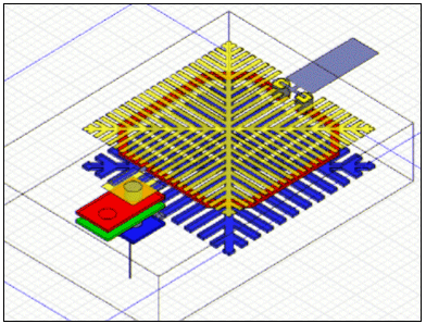
Figure 1: STMicroelectronics BGA Inductor
The model outputs are electrical performances such as inductance value (Ldiff), quality factor (Qdiff) and resonance frequency â S/Y/Z parameters [8] have been also studied to help extracting equivalent electrical model (not detailed in this paper) â.
This survey presents:
-
Inductor modeling: find an accurate analytical function linking the inductors geometrical and technological parameters to their performances.
-
Inductors synthesizing: find a robust design that fulfills with the designer requirements, including design and process variation constraints.
Modeling framework
Experiment protocol
TechModelerTM software generated 90 samples data points to cover optimally the input space parameters. For each sample, the electromagnetical simulator HFSS (from Ansoft [3]) simulated the BGA inductor for a frequency range from 0.1 to 20 GHz with a 0.1GHz increment.
In the following results of the study, 70 samples were sufficient to model efficiently the inductance. The last ones were kept for blind-validation of the models.
Checking out the design
As TechModelerTM allows an incremental generation of optimal parameters samples, we first generated 30 samples to check out the design.
The computed samples cover as well as possible the parameters space, by making all parameters independently variable for each sample. Thus, this unbiased exploration of parameters space enables a detection of design errors that is more efficient than user simulation trials. After four releases, the design has been fully corrected and is suitable for the studied range of parameters.
Refining the study
This analysis of the first data set of simulations allowed us to detect some strange simulation results (probably due to coarse grain of simulation far from the nominal frequency). We thus designed region of reliability of the simulator results by reducing the frequency range from 1 to 15 GHz. Furthermore we focus in this survey on inductor performances below the first resonance frequency.
Different output variables are modeled, such as performance values or electrical equivalent parameters. In this survey we focus on inductance value (Ldiff variable), quality factor (Qdiff variable), and resonance frequency models.
Furthermore, we limit modeling for frequency below the first resonance frequency. Some models tackle the performances strictly below the resonance, while others (as detailed in the next paragraph) take into account the first slope after resonance.
As the first resonance frequency defines the region of interest and is highly dependent on parameters, this model details are presented later in the paper.
Model performances
L and Q models including first resonance effect
The inductance value model is designed as a function of the 11 parameters (inputs) that compute the inductance value (output).
The TechModelerTM software easily tackles L value function modeling from simulation data and gives a mean relative dispersion of 2.0% on modeling data and 2.6% on validation data.
Figure 2 shows data and modeling results of inductance value. The model in this figure is drawn for one given set of design and geometrical parameter over the frequency range.
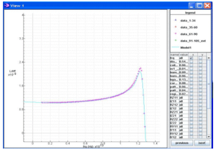

Figure 2: model of inductance value (screenshots of TechModelerTM software).
X-axis: frequency, Y-axis: Ldiff value (left and right line) with modeling data and validation data
In the same way, a quality factor model can be obtained (see Figure 3 for model curve and table 1 for dispersion results).
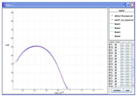
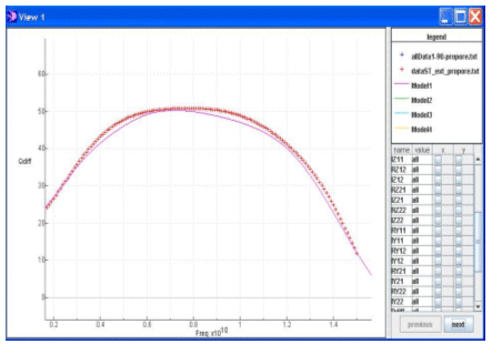
Figure 3: model of quality factor (screenshots of TechModelerTM software)
X-axis: frequency, Y-axis: Qdiff value (left and right line) with modeling data and validation data
Resonance frequency model
The modeling of the resonance frequency gives a mean relative error of 1.5% on modeling data and 2.9% on validation data. This model was computed very quickly due to his low intrinsic complexity (about 1 hour of computing time on AMD Athlon 64 2.2 GHz, 1 GB RAM).
The visualization of models for a set of various parameters allows us to see graphically the dependence of resonance frequency on some parameters. For example, Figure 4 shows clearly the effect of diameter on resonance frequency.
Note that a rigorous detailed analysis of this model controlled by many parameters can be done thanks the other InfiniScale's software TechAnalyzerTM that includes sensibility analysis taking into account random variations of input parameters.
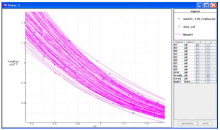
Figure 4: resonance frequency model
X-axis: diameter, Y-axis: resonance frequency
Summary of modeling results
Three models created with TechModelerTM were presented. Table 1 summarizes the goodness of fit of these models and computation time.
| model | mean relative error on modeling data | mean relative error on validation data | computation time AMD Athlon 64 â 2.2GHz 1 GB RAM |
| Ldiff (below resonance) | 0.75% | 1.6% | about 4 hours |
| Ldiff (with resonance) | 2.0% | 2.6% | about 6 hours |
| Qdiff | 6.5% | 4.8% | about 4 hours |
| res. frq | 1.5% | 2.9% | about 1 hour |
Table 1: modeling results
InfiniScale technology allowed us to perform a very fast and accurate modeling even in high dimensional parameter space (4 design parameters and 6 technological ones) and over a broad frequency range. Furthermore these modeling needed only a small number of simulations (only 70).
All the models will then be used for synthesis presented in the next section.
| Inputs | ||
| bga_y_marg | 2.000020e-01 | mm |
| bump_diam | 1.000020e-01 | mm |
| bump_height | 6.999760e-02 | mm |
| coil_width | 7.375920e-02 | mm |
| core_thick | XXXXXXXX | mm |
| diameter | 4.000000e-01 | mm |
| freq | 3.600000e+09 | Hz |
| m1_thick | XXXXXXXX | mm |
| pattern_size | 6.414450e-02 | mm |
| pattern_spac | 6.781510e-02 | mm |
| registration | 2.984660e-04 | mm |
| Outputs | ||
| Fres | 1.276351e+10 | Hz |
| Ldiff | 9.188882e-10 | H |
| Qdiff | 6.055508e+01 | |
Table 2: copied/pasted OP1 synthesis point
Synthesizing
Classical multi-objective resizing
The TechSynthesizerTM software gives the optimal inductor parameter set to reach the desired performance.
One inductor has been synthesized according to the following specifications (see table 3).
| Constraints | ||
| diameter | constrained between 0.4 and 0.45 mm | |
| freq | fixed to 3.6 GHz | |
| Ldiff | constrained by a gauge on freq | |
| at 3.3 GHz | constrained between 0.9 and 1.1 nH | |
| at 3.6 GHz | constrained between 0.9 and 1.1 nH | |
| at 3.9 GHz | constrained between 0.9 and 1.1 nH | |
| Objectives | |
| diameter | minimized |
| Qdiff | maximized |
Table 3: copied/pasted specifications of the synthesis
This specifications example shows the different kinds of constraints TechSynthesizerTM can support:
Fixed value constraints: the freq parameter has been constrained to the 3.6 GHz fixed value.
Interval constraints: the diameter parameter has been constrained to a value between 0.4 and 0.45 mm.
Gauge constraints: the Ldiff criterion is constrained for three different frequency points (3.3, 3.6 and 3.9 GHz) to a value between 0.9 and 1.1 nH.
Multi-objectives: specifications ask to minimize the diameter, and maximize the Qdiff quality factor.
TechSynthesizerTM synthesis calculation lasts a few minutes, and produces a report at the end of the process that gives the resulting synthesis point with a remind section holding the specifications attached with the given result.
The resulting synthesis point can be copied/pasted inside a document, like this article for instance (see table 2).
A rapid analysis of the resulting synthesis point can be done inside TechSynthesizerTM, plotting the output parameters as a function of one input parameter.
In the figure 5 and figure 6, the Ldiff output parameter is plotted as a function of the frequency parameter. In figure 5, input parameters of the OP1 synthesis point are given by the synthesis result. In figure 6, input parameters are the same as OP1, except for the m1_thick parameter that is increased of 10%.

Figure 5: Ldiff(freq) @ OP1

Figure 6: Ldiff(freq) @ OP1/m1_thick+10%
Synthesizing with process variations
Analyzing figure 6 shows that the resulting synthesis point is not robust regarding the metal thickness: Ldiff is out of the defined gauge when m1_thick varies of 10%.
In order to get a more robust design taking into account the process variations, it is possible to add a tolerance constraint inside the synthesis specifications:
Tolerance constraints: Ldiff and m1_thick parameters are constrained to have a tolerance of 10%.
With these two supplementary tolerance constraints, the resulting synthesis point is slightly different (see table 5):
| Inputs | ||
| bga_y_marg | 2.461300e-01 | mm |
| bump_diam | 1.078490e-01 | mm |
| bump_height | 6.986850e-02 | mm |
| coil_width | 8.221350e-02 | mm |
| core_thick | XXXXXXXX | mm |
| diameter | 4.003740e-01 | mm |
| freq | 3.600000e+09 | Hz |
| m1_thick | XXXXXXXX | mm |
| pattern_size | 6.370120e-02 | mm |
| pattern_spac | 5.902660e-02 | mm |
| registration | 2.463110e-02 | mm |
| Outputs | ||
| Fres | 1.148345e+10 | Hz |
| Ldiff | 9.200255e-10 | H |
| Qdiff | 5.707554e+01 | |
Table 5: OP2 toleranced synthesis result
We can notice that with this OP2 synthesis point, the quality factor is slightly lowered, and the Ldiff value remains quasi the same.
The tolerance analysis on m1_thick parameter gives the following results:
This analysis shows that the resulting toleranced synthesis point OP2 is now robust regarding the metal thickness: Ldiff stays inside the defined gauge when m1_thick varies of 10% (see figure 8).
To validate our synthesis results we simulated the inductor with parameters resulting from the synthesis and then compare the simulation performance with the user performance goal.

Figure 7: Ldiff(freq) @ OP2 (with process variation)

Figure 8: Ldiff(freq) @ OP2/m1_thick+10%
Synthesis results validation
Three designs have been synthesized through TechSynthesizerTM, respecting three different specific specifications. Simulations have been launched by the STMicroelectronics team for each one of these designs. The obtained Ldiff and Qdiff performances presented less than 3% dispersion between the synthesized designs and the simulated ones. This error is logically the same as the predicted mean relative error as computed with validation data during modeling step (see table 4).
| Ldiff | with 10% of tolerance |
| m1_thick | with 10% of tolerance |
Table 4: Tolerance constraints
Conclusion
In this article the InfiniScale flow for an efficient modeling and synthesis of analog devices is described, and successfully applied to the validation survey leaded by STMicroelectronics onto its new BGA inductor technology. Accurate models have been obtained using TechModelerTM software, and a robust design has been synthesized mixing both design and technological/process parameters, using TechSynthesizerTM.
Finally, the ability of this flow has been industrially approved on many analog circuits and MEMS.
References
[1] InfiniScale web site: www.infiniscale.com
[2] STMicroelectronics web site: www.st.com
[3] Ansoft corporation HFSS web site: www.ansoft.com/products/hf/hfss
[4] The spice page: bwrc.eecs.berkeley.edu/Classes/IcBook/SPICE
[5] Empirical model-building and response surfaces, G. E.P. Box, N. R. Draper, Ed. John Wiley & Sons â 1987.
[6] Plans dâexpériences : construction et analyse, D. Benoist and Y. Tourbier, Ed. Lavoisier â Tec & Doc â 1994.
[7] Plan dâexpériences pour surfaces de réponse, J. Goupy, Ed. Dunod â 1999.
[8] S-Parameter techniques, Test & Measurement application notes 95-1, Hewlett Packard
Related Semiconductor IP
- PDM Receiver/PDM-to-PCM Converter
- Voltage and Temperature Sensor with integrated ADC - GlobalFoundries® 22FDX®
- 8MHz / 40MHz Pierce Oscillator - X-FAB XT018-0.18µm
- UCIe RX Interface
- Very Low Latency BCH Codec
Related Articles
- BCD Technology: A Unified Approach to Analog, Digital, and Power Design
- Interstellar: Fully Partitioned and Efficient Security Monitoring Hardware Near a Processor Core for Protecting Systems against Attacks on Privileged Software
- Design and implementation of a hardened cryptographic coprocessor for a RISC-V 128-bit core
- Generative AI for Analog Integrated Circuit Design: Methodologies and Applications
Latest Articles
- A Scalable Open-Source QEC System with Sub-Microsecond Decoding-Feedback Latency
- SNAP-V: A RISC-V SoC with Configurable Neuromorphic Acceleration for Small-Scale Spiking Neural Networks
- An FPGA Implementation of Displacement Vector Search for Intra Pattern Copy in JPEG XS
- A Persistent-State Dataflow Accelerator for Memory-Bound Linear Attention Decode on FPGA
- VMXDOTP: A RISC-V Vector ISA Extension for Efficient Microscaling (MX) Format Acceleration