A Survey on SoC Security Verification Methods at the Pre-silicon Stage
By Rasheed Kibria, Farimah Farahmandi, and Mark Tehranipoor
Department of Electrical and Computer Engineering
University of Florida, Gainesville, FL, USA
Abstract
This paper presents a survey of the state-of-the-art pre-silicon security verification techniques for System-on-Chip (SoC) designs, focusing on ensuring that designs, implemented in hardware description languages (HDLs) and synthesized circuits, meet security requirements before fabrication in semiconductor foundries. Due to several factors, pre-silicon security verification has become an essential yet challenging aspect of the SoC hardware lifecycle. The modern SoC design process often adheres to a design reuse philosophy, integrating multiple functional blocks or Intellectual Property (IP) cores sourced from various vendors onto a single chip. While beneficial for reducing costs and accelerating time-to-market, this approach introduces numerous untrustworthy third-party entities into the supply chain. It increases the potential for introducing security vulnerabilities significantly. Additionally, hardware fabrication, assembly, and testing are frequently outsourced to third-party entities, further exacerbating security risks. Moreover, the growing complexity of SoC designs leads to unanticipated interactions between hardware and software layers, creating potential gateways for attackers to exploit and steal confidential information from devices. In response to these challenges, recent years have seen a surge in the development of innovative SoC security verification techniques. This survey provides an overview of these methods, their high-level working principles, strengths, and weaknesses. By understanding these techniques, designers can better evaluate their effectiveness and select the most appropriate methods aligned with the specific security objectives for their SoC designs.
I. INTRODUCTION
System-on-Chip (SoC) represents a platform where all electronic system components, or intellectual property (IP) blocks, are integrated into a single chip. Modern SoCs can incorporate billions of transistors within a compact area of around one hundred square millimeters. This high level of integration has made SoCs a cornerstone in modern technology and electronics. The SoC’s capability to accommodate multiple functional blocks on a single platform minimizes interface and interconnection delays, leading to superior performance compared to traditional integrated circuits [1–4]. Additionally, SoCs are cost-effective in producing, conserving energy, and saving space, further contributing to their widespread adoption. An example of a modern SoC is shown in Fig. 1, which comprises numerous IPs with diverse functionalities (analog, memory, digital, etc.).

Fig. 1: Example of a modern System-on-Chip (SoC).
The popularity of SoCs is primarily due to their versatility and efficiency. Their compact size makes them ideal for portable devices such as smartphones, cameras, tablets, and other wireless technologies. Furthermore, the ability of SoCs to be integrated into Internet of Things (IoT) devices extends their application to critical national infrastructures, including defense, finance, and transportation sectors. This adaptability enhances the functionality and reliability of these systems and underscores the significance of SoCs in advancing modern technology and maintaining critical infrastructure security and efficiency [1, 2, 5].

Fig. 2: Modern SoC design flow.
The SoC design flow is illustrated in Fig. 2. It outlines the steps in designing a modern SoC at a very high level. Due to the pressures of shrinking time-to-market and rising production costs, it has become nearly impossible for a single entity to manage the entire process of designing, developing, and fabricating an SoC independently [6–8]. Consequently, the semiconductor industry has transitioned to a horizontal model. The SoC integrator obtains IP blocks from various third-party vendors in this model [5, 7, 8]. The SoC designer then integrates these external IPs with their proprietary IPs to develop the entire SoC’s register-transfer level (RTL) description. Once the RTL code is finalized after verification, the SoC undergoes synthesis, converting the high-level design into a gate-level netlist. This netlist enters the design-for-test (DFT) insertion phase to ensure the SoC can be effectively tested for faults. Often, this phase is outsourced to specialized third-party entities due to its complexity, cost, and the need for specific expertise. After the DFT insertion, the gate-level netlist is translated into a physical layout, leading to the final GDSII file. This file is then sent to a foundry where the physical chip for the SoC is manufactured [5].

Fig. 3: Sources of security vulnerabilities in the modern SoC design flow.
In the state-of-the-art chip design lifecycle, vulnerabilities are pervasive throughout the entire SoC design process, presenting numerous potential attack surfaces. Attackers might exploit these vulnerabilities to gain unauthorized access to sensitive information once the SoC is deployed in the field. The SoC design flow often begins with defining specifications that may not be security-aware [5]. Even though these specifications are flawless, vulnerabilities can still arise during the implementation phase. Additionally, external vendors’ thirdparty intellectual property (3PIP) may contain malicious functionalities intentionally embedded by rogue employees within the design house [9–11]. Moreover, existing computer-aided design (CAD) tools used during the design translation phase prioritize optimization for area, power, and performance, often at the expense of security considerations. These tools are not equipped to address or mitigate security vulnerabilities, leaving the design susceptible to various threats [12–14]. For instance, an attacker can exploit the JTAG interface [15–17] or inject faults into the final product to execute malicious actions [18, 19]. Since SoCs are integral components in numerous computational devices, these security vulnerabilities may pose significant risks to the overall system security. In Fig. 3, the sources of potential security vulnerabilities are shown, which exist in the modern SoC design flow.

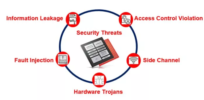
Fig. 4: Some examples of attacks on hardware.
Some examples of attack scenarios on hardware are presented in Fig. 4. These attacks may exploit the security vulnerabilities discussed earlier. Information leakage involves the unauthorized disclosure of confidential information to untrusted entities. This leakage can be intentionally introduced by third-party intellectual property (3PIP) vendors or unintentionally induced by computer-aided design (CAD) tools [20– 22]. Inherent hardware vulnerabilities, such as specification flaws or weak implementations, can be exploited through fault injection techniques. Attackers may use methods like power or clock glitches, temperature variations, and light, laser, or electromagnetic emissions to induce faults in the hardware [18, 19, 23–25]. These faults can lead to the leakage of sensitive information, including cryptographic keys, user credentials, and passwords, or result in the unwanted modification of security-critical data, compromising the system’s confidentiality and integrity. Hardware Trojans represent another significant threat, involving malicious changes to the design by rogue employees within the design house or foundry. These Trojans are intentionally embedded to leak secret information (resulting in confidentiality violations) or to alter sensitive data (leading to integrity violations) [9–11]. Side-channel attacks pose a unique challenge as they do not require any design modification. Instead, they exploit covert channels or physical parameters, such as power consumption, electromagnetic emissions, or timing information, to extract sensitive information [26–28]. Additionally, attackers may exploit designfor- test (DFT) and design-for-debug (DFD) structures, such as scan chains, compression, and JTAG interfaces, to gain unauthorized access to the design [15–17, 29]. By maliciously exploiting these structures’ controllability and observability features, attackers can violate access controls, undermining the security of the SoC.

Fig. 5: Relative cost of design modification: Rule of 10.
A comprehensive security verification methodology must be adopted to address potential security vulnerabilities and threats effectively. This security verification process should begin at the earliest stages of the SoC design lifecycle to ensure the timely detection and mitigation of security issues [1, 2, 12]. Early-stage security verification is crucial because addressing vulnerabilities becomes significantly more challenging and costly as the design progresses. During the post-silicon stages, designers have limited flexibility to update or modify the SoC design, making it quite difficult to resolve security issues that originate from earlier design phases. The economic implications of performing security verification at the later stages of the SoC design lifecycle are underscored by the Rule of 10. It states that modifying a design at later stages of the SoC design flow is ten times more expensive than making changes during earlier stages [1, 2, 12, 30]. A pictorial representation of this notion is shown in Fig. 5. This principle highlights the exponential cost increase associated with identifying and fixing security vulnerabilities during the later design and fabrication R. KIBRIA et al.: A Survey on SoC Security Verification Methods at the Pre-silicon Stage 3 processes. By integrating security verification at the initial stages of the SoC design lifecycle, designers can ensure that vulnerabilities are addressed promptly and effectively, thereby enhancing the security of the final product. Specifically, the primary objectives of this paper are as follows-
- Providing an overview of the state-of-the-art security verification methodologies for SoC designs;
- Discussing various types of vulnerability identification techniques at the pre-silicon stage of the design lifecycle;
- Assessing the advantages and limitations of the techniques, providing their effectiveness in identifying potential security issues during the SoC design process.
The rest of the paper is organized as follows. Section II provides a detailed overview of the challenges and limitations associated with traditional security verification methods. It also presents a high-level overview of state-of-the-art SoC security verification techniques. Section III is focused on code review-based techniques for identifying potential security vulnerabilities present in the RTL codes of an SoC. Section IV presents the security property-based formal verification methodology and its advantages and limitations. Section V illustrates the dynamic security verification methods such as penetration and fuzz testing with their pros and cons. Finally, in Section VI, we conclude with the summary of this survey.
To read the full article, click here
Related Semiconductor IP
- JESD204E Controller IP
- eUSB2V2.0 Controller + PHY IP
- I/O Library with LVDS in SkyWater 90nm
- 50G PON LDPC Encoder/Decoder
- UALink Controller
Related Articles
- A Survey on the Design, Detection, and Prevention of Pre-Silicon Hardware Trojans
- IC design: A short primer on the formal methods-based verification
- A closer look at security verification for RISC-V processors
- Interstellar: Fully Partitioned and Efficient Security Monitoring Hardware Near a Processor Core for Protecting Systems against Attacks on Privileged Software
Latest Articles
- Crypto-RV: High-Efficiency FPGA-Based RISC-V Cryptographic Co-Processor for IoT Security
- In-Pipeline Integration of Digital In-Memory-Computing into RISC-V Vector Architecture to Accelerate Deep Learning
- QMC: Efficient SLM Edge Inference via Outlier-Aware Quantization and Emergent Memories Co-Design
- ChipBench: A Next-Step Benchmark for Evaluating LLM Performance in AI-Aided Chip Design
- COVERT: Trojan Detection in COTS Hardware via Statistical Activation of Microarchitectural Events