A Guide on Logical Equivalence Checking - Flow, Challenges, and Benefits
By Pratik Patel, Prathmesh Oza and Rakesh Parmar (eInfochips)
Introduction
The VLSI design cycle is divided into two phases: Front-end and Back-end. Front-end covers the architectural specifications, coding and verification, whereas back-end involves the physical implementation of the design on the targeted technology node.
This paper presents why LEC (Logical Equivalence Check) is important in the ASIC design cycle, how to check it, and what to do when LEC is failing. We will explore a test case to see what happens if LEC fails – how to pinpoint the problem and what steps to take for resolving the same.
Importance of LEC
- Design passes through various steps like synthesis, place and route, sign-offs, ECOs (engineering change orders), and numerous optimizations before it reaches production. At every stage, we need to make sure that the logical functionality is intact and does not break because of any of the automated or manual changes. If the functionality changes at any point during the entire process, the entire chip becomes useless. This is why LEC is one of the most important checks in the entire chip design process.
- With shrinking technology nodes and increasing complexity, logical equivalence check plays a major role in ensuring the correctness of the functionality.
LEC comprises of three steps as shown below: Setup Mode, Mapping Mode and Compare Mode.

Fig-1. Logical Equivalence Check flow diagram
There are various EDA tools for performing LEC, such as Synopsys Formality and Cadence Conformal. We are considering Conformal tool as a reference for the purpose of explaining the importance of LEC.
Steps for Logical Equivalence Checks
Let’s take a close look at the various steps of logical equivalence checks:
1) Setup
In the setup mode, the Conformal tool reads two designs. We designate the design types, which are Golden (synthesized netlist) and Revised (generally, the revised design is the modified or post-processed design that the Conformal tool compares to the Golden design). For the execution of LEC, the Conformal tool requires three types of files.
- <design_name>.lec file guide the Conformal tool to execute different command in a systematic way.
- <design_name>.scan_const file provides scan related constraints like if we want to ignore some scan connections/serdes input/output pins which are defined in this file.
- <design_name>.stdlib file contains pointer of standard cells library.
In the transition from setup mode to LEC mode, the Conformal tool flattens and models the golden and revised designs and automatically maps the key points. The key points are defined as:
- Primary Inputs
- Primary Outputs
- D Flip-Flops
- D Latches
- TIE-E Gates (error gate, created when x-assignment exists in revised design)
- TIE-Z Gates (high impedance or floating signals)
- Black boxes
2) Mapping
During the second phase of equivalence checking, the Conformal tool automatically maps key points and compares them. When the comparison is complete, it pinpoints the differences. The Conformal tool employs two name-based methods and one no-name method to map key points. Name-based mapping is useful for gate-to-gate comparisons when minor changes have been made to the logic.
Conversely, the no-name-mapping method is useful when the Conformal tool must map designs with completely different names. By default, it automatically maps key points with the name-first mapping method when it exits the setup mode. The key points that the Conformal tool does not map are classified as unmapped points.
Unmapped points are classified into three categories:
- Extra unmapped points are key points that are present in only one of the designs, Golden or Revised.
- Unreachable unmapped points are key points that do not have an observable point, such as a primary output.
- Not-mapped unmapped points are key points that are reachable but do not have a corresponding point in the logic fan-in cone of the corresponding design.
3) Compare
After the Conformal tool maps the key points, the next step of the verification is comparison. Comparison examines the key points to determine if they are equivalent or non-equivalent. The comparison determines if the compared points are:
- Equivalent
- Non-equivalent
- Inverted-equivalent
- Aborted
In the case of aborted compare points, we can change the compare effort to a higher setting. Thus, the Conformal tool can continue the comparison on only the aborted compare points. The Conformal tool displays the completed run time and total memory used for the comparison.
Multiple reports are generated once LEC is completed:
- Non-equivalence report
- Unmapped report
- Blockbox report
- Abort.rpt
- Unreachable.rpt
- Floating.rpt
- Mapped.rpt
At the time of sign-off or tapeout phase, the schedule is too tight to handle blocks with some critical logical failure. At times, the logical connectivity is broken while doing manual fixes or timing ECOs. The chances of a logical breakdown will be high at the tapeout phase where the physical design engineer does not have much time for block closure. Also, the chances of breaking logical connectivity are high, when you get the functional ECO and do the manual connection. Let’s take a look at a practical example of LEC failure in a block and see how it can be solved.
Sample case
First of all, do not panic if LEC fails during any of the levels, discussed earlier. When LEC is failing, the first step is to check the "non-equivalent.rpt” file. It may be possible that due to one broken connection, a higher number of cell names are reported in the "non-equivalent.rpt" file.
The reason behind is that many paths which are going through one failed/broken connection – and hence all its endpoints (compare points) – are reported “Non-equivalent”.
Step 1: Non-equivalent Report
The first step is to check the non-equivalent file. The sample non-equivalent file below shows the 152 compare points that are failing in in LEC.


These 152 flip-flops reported as non-equivalent are the multibit flops. In multibit flops, we merge two flops to form a single flop having multiple input and output pins. For example, if we merge two single bit flops into one multibit flop, it will have D0,D1 as input pins and Q0,Q1 as output pins.

Because of multibit flops, the report is showing 152 flop count as non-equivalent, but actually only 72 are non-equivalent. As these are two bit flops, the total count is 72x2=144 flops. The remaining are single bit flops.
Step-2: Unmapped Report
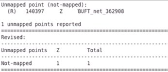
Next step is to check the unmapped file. This file shows the unmapped nets where the logical connectivity is broken. We need to trace nets and find out the missing connection of those nets.

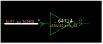
In the above image, we can see that one net (BUFT_net_362908) is not mapped in the design. As it can be seen in Fig-2, once we check this net (BUFT_net_362908) connection in LEC fail database, we see that it is connected only to the input pins of other cell (*_364714/A), but the other connection (driver side) of this net is missing due to unintentional cell deletion.
The highlighted net in the below figure shows the net reported in the unmapped.rpt file.

Fig-2. Net reported in unmapped report
Here, we can see the connection of reported net in the LEC fail design.
![]()
While we do the fanout of net (BUFT_net_362908) which is reported in unmapped file, it is connected to 152 flops in LEC pass database.
![]()
Whereas 152 flops reported in non-equivalent file in LEC fail database are same as fanout of net (BUFT_net_362908) reported in LEC pass database.

Now, we need to find the actual net connection of this net in the previous LEC pass database. While checking, we can easily note that the reported net is connected to one inverter which is missing in the LEC fail database.
For finding the missing cell, we have to back trace this net in the previously LEC passed database and check actual connections.

Do not get confused between un-mapped and non-equivalent reports. In the un-mapped report we only see the floating nets of the undriven input pins, whereas in the non-equivalent report we see all the cells which are fanouts of this missing cell.
Step 3: Fix the LEC Issue
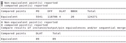
After finding the reason for the LEC failure, we have to insert one missing inverter and redo the input/output logical connection of this inverter in the LEC failed database. Fig-3 shows the newly added inverter and its input-output connection. Now, if we rerun the LEC it will pass and non-equivalent report will show zero non-equivalent points.

Fig-3. Fix the missing connection

Common areas where LEC fail
- If multibit flops are used in the design, then the issue of mapping golden netlist versus revised netlist will crop up, as flop names will be changed in revised netlist.
- Clock gating cells not getting mapped after cloning in revised netlist.
- Logical connectivity breaks during timing fixing or while doing manual ECO.
- Functional ECO implementation.
- Missing DFT constraints.
Benefits of LEC
- Less reliance on gate level simulation.
- Boosted confidence in new tool revisions for synthesis and place & route.
- Watch-dog for poor RTL coding areas in the design.
- Nearly exhaustive proof of equivalence without writing test patterns.
- Decreased risk of missing bugs inserted by the back-end process.
Conclusion
This paper gives an introduction of logical equivalence check, flow setup, steps to debug it, and solutions to fix LEC. Using a real-world scenario, it also showcases the reports generated after LEC completion and suggests an easy way to find out the root cause of LEC failure. It is not uncommon for teams to run into LEC fail issues – simply taking the steps described in this paper will help you resolve the issues related to LEC.
References
http://www.europractice.stfc.ac.uk/vendors/cadence_encounter_conformal_EC2012_ds.pdf
About the Authors
Pratik Patel is a Senior Physical Design Engineer at eInfochips. With over 4 years of experience in lower technology node for complex networking SoCs, he has developed expertise in PnR, static timing analysis and power optimization.
Prathmesh Oza is a Senior Physical Design Engineer at eInfochips. He holds a Bachelor of Engineering degree in Electronics and Communication from Charotar institute of Technology, India. With over 5+ years of experience in lower technology node for complex networking SoCs, he is an expert in PnR, STA analysis and power optimization.
Rakesh Parmar is an ASIC technical manager at eInfochips. He holds a Master's degree in Electronics from Sardar Patel University, India. Leveraging a decade of experience in technology domain and physical design, he is now focusing on delivering complex SOC ASIC products in lower technology nodes for eInfochips’ customers.
Related Semiconductor IP
- NPU IP Core for Mobile
- NPU IP Core for Edge
- Specialized Video Processing NPU IP
- HYPERBUS™ Memory Controller
- AV1 Video Encoder IP
Related White Papers
- Understanding Logic Equivalence Check (LEC) Flow and Its Challenges and Proposed Solution
- Interstellar: Fully Partitioned and Efficient Security Monitoring Hardware Near a Processor Core for Protecting Systems against Attacks on Privileged Software
- A Survey on the Design, Detection, and Prevention of Pre-Silicon Hardware Trojans
- Sequential equivalence checking supports ESL flow
Latest White Papers
- Ramping Up Open-Source RISC-V Cores: Assessing the Energy Efficiency of Superscalar, Out-of-Order Execution
- Transition Fixes in 3nm Multi-Voltage SoC Design
- CXL Topology-Aware and Expander-Driven Prefetching: Unlocking SSD Performance
- Breaking the Memory Bandwidth Boundary. GDDR7 IP Design Challenges & Solutions
- Automating NoC Design to Tackle Rising SoC Complexity