SEMI Reports Shift in Semiconductor Capacity and Equipment Spending Trends
SAN JOSE, Calif. — January 9, 2014 — Based on SEMI World Fab Forecast data, SEMI suggests that spending trends for the semiconductor industry have changed. Before 2009, capacity expansion corresponded closely to fab equipment spending. Now more money is spent on upgrading existing facilities, while new capacity additions are occurring at a lower pace, to levels previously seen only during an economic or industry-wide slowdown.
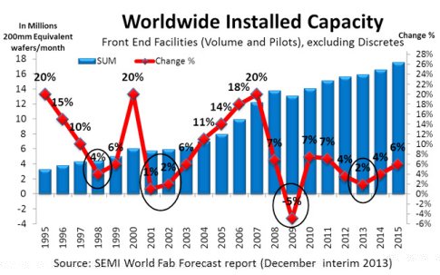
While the 2013 installed capacity growth mimics economic crisis behavior, according to the SEMI World Fab Forecast Report, the data support improvement in overall capacity expansion in both 2014 and 2015.
Figure 1: Installed Capacity for Front End Facilities over time (without Discretes)

Most fab equipment spending before the 2009 crisis focused on adding new capacity. In the five years between 2003 and 2007, the annual growth rate of new capacity increased from 6 percent in 2003 to 20 percent growth in 2007 (almost doubling the fab capacity in five years), according to the SEMI World Fab Forecast Report. This was driven mainly by DRAM and NAND companies in Korea, Taiwan and China. After 2009, while fab equipment spending recovered, new capacity additions trended below pre-2009 growth rates: growth of new capacity dropped from 7 percent in 2010 to about 4 percent in 2014, with the expected capacity addition of only 17 percent in the five years from 2009 to 2014.
Since the 2009 crisis, expenditures on upgrading existing equipment have grown sharply. Expansion projects, such as new fabs, still account for the majority of fab equipment spending, but in lower proportions than in the past. Costs for adding new equipment to a new facility are typically higher than upgrading some of the existing equipment.
According to SEMI, the two industry segments predicted to add the most capacity in 2013 and 2014, based on demand, are foundries and NAND. Dedicated foundries grew at a steady 10 percent in 2013, and will add another 8 to 10 percent in 2014. For the second largest segment, NAND, which lost about 4 percent of capacity in 2012, capacity rose 10 percent in 2013 and will add another 5 to 8 percent in 2014. Other segments, such as DRAM, Analog, and Logic, are not expected to add new capacity in 2013 and 2014. MPU may add some new capacity by 2014. For more information, visit www.semi.org/MarketInfo/FabDatabase.
Learn more about the data in the SEMI World Fab Forecast (www.semi.org/en/Store/MarketInformation/fabdatabase/ctr_027238) which lists about 1,150 facilities. Sixty-seven of these have started or will start volume production in 2013 or later. The report lists major investments (construction projects and equipping) in 206 facilities and lines in 2013, and 180 facilities and lines in 2014. The forecast uses a bottom-up approach methodology, providing high-level summaries and graphs, and in-depth analyses of capital expenditures, capacities, technology and products by fab. These tools are invaluable for understanding how the semiconductor manufacturing will look in 2013 and 2014, and learning more about capex for construction projects, fab equipping, technology levels, and products.
The SEMI Worldwide Semiconductor Equipment Market Subscription (WWSEMS) data tracks only new equipment for fabs and test and assembly and packaging houses. The SEMI World Fab Forecast and its related Fab Database reports track any equipment needed to ramp fabs, upgrade technology nodes, and expand or change wafer size, including new equipment, used equipment, or in-house equipment. Learn more about the SEMI fab databases at www.semi.org/MarketInfo/FabDatabase and www.youtube.com/user/SEMImktstats
About SEMI
SEMI is the global industry association serving the nano- and microelectronics manufacturing supply chains. Our 1,900 member companies are the engine of the future, enabling smarter, faster and more economical products that improve our lives. Since 1970, SEMI has been committed to helping members grow more profitably, create new markets and meet common industry challenges. SEMI maintains offices in Bangalore, Beijing, Berlin, Brussels, Grenoble, Hsinchu, Moscow, San Jose, Seoul, Shanghai, Singapore, Tokyo, and Washington, D.C. For more information, visit www.semi.org.
Related Semiconductor IP
- UCIe D2D Adapter & PHY Integrated IP
- Low Dropout (LDO) Regulator
- 16-Bit xSPI PSRAM PHY
- MIPI CSI-2 CSE2 Security Module
- ASIL B Compliant MIPI CSI-2 CSE2 Security Module
Related News
- SEMI Projects Double-Digit Growth in Global 300mm Fab Equipment Spending for 2026 and 2027
- Fab Equipment Spending Breaking Industry Records
- Semiconductor Equipment Record Spending Streak To Continue Through 2019
- Total Fab Equipment Spending Reverses Course, Growth Outlook Revised Downward
Latest News
- Wind River Joins the CHERI Alliance and Collaborates with Innovate UK to Accelerate Cybersecurity Innovation
- Arteris and MIPS Partner to Accelerate Development for Physical AI Platforms
- DCD-SEMI expands CryptOne with EdDSA Curve25519 IP core for secure embedded systems
- Syntacore's SCR RISC-V IP Now Supports Zephyr 4.3
- Xylon Presents New 12-Channel GMSL3/GMSL2 FMC+ ExpansionBoard