New Fabs Invest Over $220 Billion; 2019 to Mark All-Time Spending High
MILPITAS, Calif. – September 17, 2018 – Global fab equipment spending will increase 14 percent this year to US$62.8 billion and is expected to rise 7.5 percent, to US$67.5 billion, in 2019, marking the fourth consecutive year of spending growth and the highest investment year for fab equipment in the history of the industry, according to the latest World Fab Forecast Report published today by SEMI. Investments in new fab construction are also nearing a record with a fourth consecutive year of growth predicted and capital outlays next year approaching US$17 billion.
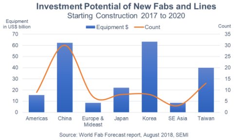
Investments for fab technology and product upgrades, as well as for additional capacity, will grow as the emergence of numerous new fabs significantly increases equipment demand, the forecast shows. The World Fab Forecast Report currently tracks 78 new fabs and lines that have or will start construction between 2017 to 2020 (with various probabilities) and will eventually require more US$220 billion in fab equipment (Figure 1). Construction spending for these fabs and lines is expected to reach US$53 billion during this period.

Figure 1: Shows the investment potential of new fabs and lines starting construction between 2017 and 2020.
Korea is projected to lead other regions in fab equipment investments with US$63 billion, US$1 billion more than second-place China. Taiwan is expected to claim the third spot at US$40 billon, followed by Japan at US$22 billion and the Americas at US$15 billion. Europe and Southeast Asia will share sixth place, with investments totaling US$8 billion each. Fully 60 percent of these fabs will serve the Memory sector (the lion’s share will be 3D NAND), and a third will go to Foundry.
Of the 78 fab construction projects starting construction between 2017 and 2020, 59 began construction in the first two years (2017 and 2018), while 19 are expected to begin in the last two years (2019 and 2020) of the tracking period.
Equipping a new fab typically takes one to one and a half years, though some fabs take two years and others longer, depending on various factors as such the company, fab size, product type and region. Approximately half of the projected US$220 billion will be spent from 2017 and 2020, with less than 10 percent invested in 2017 and 2018, nearly 40 percent in 2019 and 2020, and the rest after 2020.
While the US$220 billion estimate is based on current insights of known and announced fab plans, total spending could exceed this level as many companies continue to announce plans for new fabs. Since the last quarterly publication of the report published last quarter, 18 new records – all new fabs – have been added to the forecast. Up-to-date and detailed analysis, with a bottoms-up approach, is available by subscribing to SEMI’s World Fab Forecast Report.
Since its June 1 publication, more than 340 updates have been made to the World Fab Forecast. The report now includes more than 1,200 records of current and future front-end semiconductor facilities from high-volume production to research and development. The report covers data and predictions through 2019, including milestones, detailed investments by quarter, product types, technology nodes and capacities down to fab and project level.
Learn more about the SEMI fab databases at www.semi.org/en/MarketInfo/FabDatabase.
About SEMI
SEMI® connects over 2,000 member companies and 1.3 million professionals worldwide to advance the technology and business of electronics manufacturing. SEMI members are responsible for the innovations in materials, design, equipment, software, devices, and services that enable smarter, faster, more powerful, and more affordable electronic products. FlexTech, the Fab Owners Alliance (FOA) and the MEMS & Sensors Industry Group (MSIG) are SEMI Strategic Association Partners, defined communities within SEMI focused on specific technologies. Since 1970, SEMI has built connections that have helped its members prosper, create new markets, and address common industry challenges together. SEMI maintains offices in Bangalore, Berlin, Brussels, Grenoble, Hsinchu, Seoul, Shanghai, Silicon Valley (Milpitas, Calif.), Singapore, Tokyo, and Washington, D.C. For more information, visit www.semi.org.
Related Semiconductor IP
- Low Dropout (LDO) Regulator
- 16-Bit xSPI PSRAM PHY
- ASIL B Compliant MIPI CSI-2 CSE2 Security Module
- SHA-256 Secure Hash Algorithm IP Core
- EdDSA Curve25519 signature generation engine
Related News
- Andes Technology Announces over 10 Billion Cumulative Shipments of Andes-Embedded SoCs and Records All-Time High Annual and Monthly Revenue in 2021
- Global Fab Equipment Spending Forecast to Reach All-Time High of Nearly $100 Billion in 2022, SEMI Reports
- Semiconductor Fabs to Log Record Spending of Nearly $68 Billion in 2021 After 2020 Lull, SEMI Reports
- Global Fab Equipment Spending Projected to Reach New High of Nearly $100 Billion in 2022, SEMI Reports
Latest News
- Analog Bits Demonstrates Real-Time On-Chip Power Sensing and Delivery on TSMC N2P Process at TSMC 2026 Technology Symposiums
- TES offers a High-Frequency Synthesizer and Clock Generator IP for X-FAB XT018 - 0.18µm BCD-on-SOI technology
- Faraday Delivers IP Solutions to Enable Endpoint AI Based on UMC’s 28nm SST eFlash
- AiM Future Partners with Metsakuur Company to Commercialize NPU-Integrated Hardware
- ESD Alliance Reports Electronic System Design Industry Posts $5.5 Billion in Revenue in Q4 2025