TechInsights - The much anticipated Intel 14 nm is finally here!
OTTAWA, Ontario, Nov. 5, 2014 -- TechInsights, the global leader in semiconductor technical analysis, intellectual property consulting and patent brokerage services, is analyzing the Intel 5Y70 processor fabricated using Intel's state-of-the-art 14 nm Tri-gate (finFET) CMOS process.
Our soon to be published reports, Detailed Structural Analysis and Multi-Temperature Transistor Characteristics of the Intel 14 nm 5Y70 Processor, will provide both a comprehensive analysis of the structures and materials used to fabricate the device, along with the electrical performance characteristics of the core logic NMOS and PMOS transistors.
Intel debuted its finFET process with its 22 nm node IVY Bridge Processor in 2012, a market first at the time; and Intel remains the only foundry with a full production finFET CMOS process. Intel rightly claims its 2nd generation finFET process with the introduction of the Core-M series of processors, including the Broadwell based 5Y70 processor.
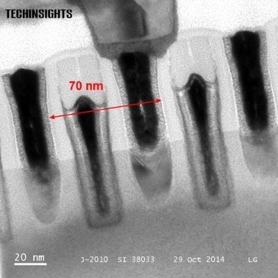
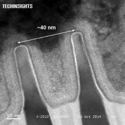
The 5Y70 features Intels 14 nm node finFET transistors having a 70 nm contacted gate pitch, sub-42 nm fin pitch, sub-60 nm pitch metal interconnects and sub 0.06 µm2 6T SRAM cell. Air gaps between densely packed metal lines are used for the first time in a logic process.
.

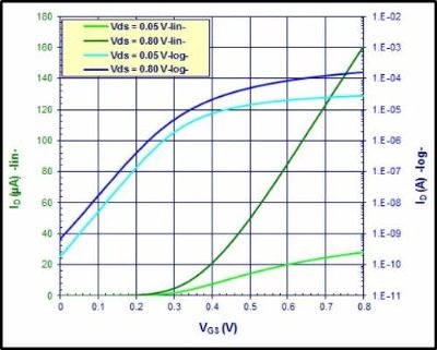
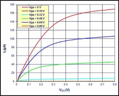
Preliminary sample data from the single temp TC analysis is shown below. The first plot is the transfer characteristics (Id vs. Vgs), the second plot is the family of curves (Id vs. Vds) for the logic NMOS transistors.
View gallery
.
.
Foundries rarely disclose the details of their technologies, making TechInsights structural analysis and transistor characterization reports a critical tool for benchmarking purposes. TechInsights' has analyzed Intel's process technologies since 1995 offering valuable insight into their Processor Roadmap. Over the past decade, Intel developed both CPU and SoC processes to maintain their lead in the PC/server markets and penetrate mobile applications. Their 45 nm Atom processor may have been the first salvo in the mobile space, with the intent being reiterated with their 22 nm node Valleyview SoC. There can be no doubt about Intel's intention to be a major supplier to the mobile and laptop/ table markets at the 14 nm node.
Intel has a wide variety of products (processors and SoC's) requiring different designs at each particular technology node. SoC products often incorporate passive components (resistors, capacitors and inductors) that are often not seen in regular CPU products.
TechInsights Structural Analysis and Transistor Characteristics reports provide key insights into Intel's manufacturing technologies used in their industry leading 14 nm Tri-gate p5Y70 processor.
About TechInsights
We possess the world's most comprehensive technical body of knowledge gained from a quarter century of reverse engineering excellence in semiconductors, electronics and software. Our experts in understanding and mapping technology to patents have helped clients, including over half of the top 50 US patent holders, get the most from their IP assets. TechInsights helps IP owners maximize the value of their patents through portfolio assessment, understanding cross-market applicability and advising on development, assertion and divestment strategies. If you need assistance in managing your most complex technology or IP challenges, turn to TechInsights for assured results. To learn more, visit www.techinsights.com
Related Semiconductor IP
- SHA-256 Secure Hash Algorithm IP Core
- EdDSA Curve25519 signature generation engine
- DeWarp IP
- 6-bit, 12 GSPS Flash ADC - GlobalFoundries 22nm
- LunaNet AFS LDPC Encoder and Decoder IP Core
Related News
- Altera to Build Next-Generation, High-Performance FPGAs on Intel's 14 nm Tri-Gate Technology
- Altera Achieves Industry Milestone: Demonstrates FPGA Technology Based on Intel 14 nm Tri-Gate Process
- Altera Enables Customer Design Starts for 14 nm Stratix 10 FPGAs and SoCs
- Samsung Delivers Its 14 nm
Latest News
- Omnitrx introduces Omni500 Ethernet Evaluation Platform, Built on Comcores Expertise
- Three Misconceptions About the $402B Semiconductor Foundry Industry
- TSMC March 2026 Revenue Report
- CoreHW Expands RTLS Portfolio with All-in-One CoreRTLS Software Platform
- Rapidus Opens Analysis Center and Rapidus Chiplet Solutions