CEA-Leti and Fraunhofer IPMS Validate Wafer Exchange for Ferroelectric Memory Materials Within the FAMES Pilot Line
Successful HZO Ferroelectric Wafer Loops Confirm Functionality Across FAMES Sites, And Advance Europe’s Collaborative Platform for Next-Generation Non-Volatile Memory
GRENOBLE, France and DRESDEN, Germany — March 23, 2026 — CEA-Leti and Fraunhofer IPMS have successfully completed the first exchange of ferroelectric memory wafers within the FAMES Pilot Line, marking a pivotal milestone in establishing a shared European platform for advanced embedded non-volatile memory (NVM) technologies. Launched in December 2023 and coordinated by CEA-Leti, the five-year initiative has demonstrated the viability of circulating complex material stacks across some of its leading research fabs.
The collaboration initially focused on the processing and electrical characterization of hafnium-zirconium oxide (HZO) ferroelectric capacitor stacks. Utilizing the combined 300 mm CMOS cleanroom capabilities of both institutes, they circulated the wafers in short process loops to enable joint evaluation of materials, electrode configurations, and device behavior.
The work also validated the wafer exchange and contamination-control protocols implemented in the pilot line, demonstrating that complex material stacks can be processed reliably across multiple advanced semiconductor facilities across all wafers.
The entire process adhered to standardized contamination control procedures, verified through VPD-ICP-MS (Vapor Phase Decomposition – Inductively Coupled Plasma Mass Spectrometry) and TXRF (Total Reflection X-Ray Fluorescence) analytics. Devices were evaluated using a ferroelectric capacitor (FeCAP) array test vehicle designed by CEA-Leti, with electrical characterization performed via the PUND (Positive-Up-Negative-Down) methodology to isolate true ferroelectric switching from parasitic effects.
‘Critical Insights’
"The successful wafer exchange marks an important step toward a joint European material-testing platform for ferroelectric memories," said Dr. Wenke Weinreich, Division Director of Fraunhofer IPMS’ Center Nanoelectronic Technologies, a member of the 11-member FAMES consortium. "By combining our processing expertise with CEA-Leti’s CMOS integration capabilities, the pilot line provides a powerful environment for evaluating new ferroelectric stacks and accelerating their path toward system-level applications."
Initial experimental results have already yielded critical insights. The team screened various electrode materials to enhance performance, finding that titanium nitride (TiN) bottom electrodes significantly outperform tungsten. In reliability tests, TiN exhibited lower failure rates after 10⁷ field cycles at 4 MV/cm. Furthermore, clear cross-split effects were observed across different electrode configurations, confirming the sensitivity of the test vehicles to process variations.
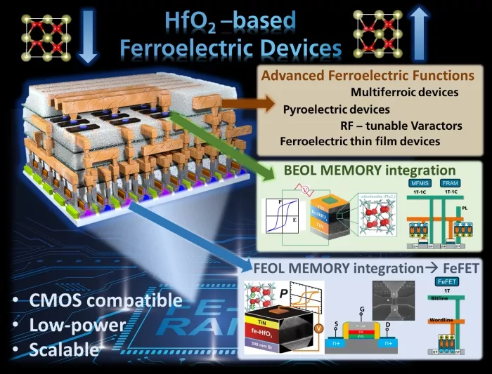
Illustration of HfO₂-based ferroelectric devices enabling scalable, CMOS-compatible NVM. The architecture supports integration in both front-end (FeFET) and back-end memory structures, while opening pathways to advanced ferroelectric functionalities such as multiferroic, pyroelectric, and tunable RF devices. © Fraunhofer IPMS
Seamless Wafer Exchanges Across FAMES Sites
"This first exchange between CEA-Leti and Fraunhofer IPMS demonstrates that shared process flows, test vehicles, and characterization environments can work seamlessly across FAMES sites," noted Dominique Noguet, pilot line coordinator and CEA-Leti vice president. "Establishing reliable wafer loops between leading research fabs is essential for accelerating ferroelectric memory development."
Looking ahead, the wafer loops lay the groundwork for broader collaborative development. Upcoming phases will integrate HfO₂-based ferroelectric stacks from Fraunhofer IPMS into CEA-Leti CMOS processes, followed by array-level evaluations on GlobalFoundries' 22nm FDX® Memory Advanced Demonstrator Multi-Project Wafer shuttle prepared by CEA-Leti. This builds on Fraunhofer IPMS' recent completion of a first chip tape-out using the same 22nm FDX® technology, which also initiated research on algorithm-based AI compute-in-memory accelerator architectures. The roadmap further includes studies on electrode process variations, long-term reliability, and back-end-of-line (BEOL) integration approaches, such as nanosecond laser annealing (NLA).
Together, these efforts advance the core mission of the FAMES Pilot Line: to provide a unified European platform for developing and validating emerging memory technologies—including OxRAM, MRAM, FeRAM, and FeFET. By enabling collaborative material development and standardized characterization, the initiative aims to strengthen Europe’s capacity to design and manufacture the low-power, next-generation chip architectures required for the future of computing.

About Fraunhofer IPMS
Fraunhofer IPMS is a leading international research and development service provider for electronic and photonic microsystems in the fields of intelligent industrial solutions, medical technology and health, mobility, and green and sustainable microelectronics. Its research focuses on customer-specific miniaturized sensors and actuators, MEMS systems, microdisplays, and integrated circuits, as well as wireless and wired data communication. Its services range from consulting and design to process development and pilot series production. With the Center Nanoelectronic Technologies (CNT), Fraunhofer IPMS offers applied research on 300 mm wafers for microchip producers, suppliers, device manufacturers and R&D partners.
Visit https://www.ipms.fraunhofer.de/en.html
About CEA-Leti
CEA-Leti, a technology research institute at CEA, is a global leader in miniaturization technologies enabling smart, energy-efficient and secure solutions for industry. Founded in 1967, CEA-Leti pioneers micro-& nanotechnologies, tailoring differentiating applicative solutions for global companies, SMEs and startups. CEA-Leti tackles critical challenges in healthcare, energy and digital migration. From sensors to data processing and computing solutions, CEA-Leti’s multidisciplinary teams deliver solid expertise, leveraging world-class pre-industrialization facilities. With a staff of more than 2,000 talents, a portfolio of 3,200 patents, 14,000 sq. meters of cleanroom space and a clear IP policy, the institute is based in Grenoble (France) and has offices in San Francisco (United States), Brussels (Belgium), Tokyo (Japan), Seoul (South Korea) and Taipei (Taiwan). CEA-Leti has launched 80 startups and is a member of the Carnot Institutes network. Follow us on www.leti-cea.com and @CEA_Leti.
Technological expertise
CEA has a key role in transferring scientific knowledge and innovation from research to industry. This high-level technological research is carried out in particular in electronic and integrated systems, from microscale to nanoscale. It has a wide range of industrial applications in the fields of transport, health, safety and telecommunications, contributing to the creation of high-quality and competitive products.
For more information: www.cea.fr/english
About FAMES Pilot Line
FAMES (FD-SOI Pilot Line for Applications with embedded non-volatile Memories, RF, 3D Integration & PMIC, to ensure European Sovereignty) gathers leading RTOs and academic partners to develop five key technologies and an eco-innovation program that will enable new chip architectures. The project includes an open access program to enable semiconductor stakeholders to gain access to the Pilot Line and the FAMES technologies, and a comprehensive training program.
Related Semiconductor IP
- SHA-256 Secure Hash Algorithm IP Core
- EdDSA Curve25519 signature generation engine
- DeWarp IP
- 6-bit, 12 GSPS Flash ADC - GlobalFoundries 22nm
- LunaNet AFS LDPC Encoder and Decoder IP Core
Related News
- NY CREATES and Fraunhofer Institute Announce Joint Development Agreement to Advance Memory Devices at the 300mm Wafer Scale
- Fraunhofer IPMS develops new 10G TSN endpoint IP Core for deterministic high-speed Ethernet networks
- Fraunhofer IPMS collaborates with Korean TSN Lab to further develop IP solutions for automotive and industrial connectivity
- CAN FD Plug Fest Shows Robust Operation of Controller IP Core by CAST and Fraunhofer IPMS
Latest News
- ESD Alliance Reports Electronic System Design Industry Posts $5.5 Billion in Revenue in Q4 2025
- Omnitrx introduces Omni500 Ethernet Evaluation Platform, Built on Comcores Expertise
- Three Misconceptions About the $402B Semiconductor Foundry Industry
- TSMC March 2026 Revenue Report
- CoreHW Expands RTLS Portfolio with All-in-One CoreRTLS Software Platform